Memory rank decoder for a multi-rank Dual Inline Memory Module (DIMM)

a dual-rank, memory rank decoding technology, applied in the field of memory rank decoding for a dual-rank inline memory module (dimm), can solve the problems of increasing the load of the dq-data bus, limiting the number m of memory ranks, and deteriorating the rate of data signals connected to each dq data bus

Active Publication Date: 2007-09-04
POLARIS INNOVATIONS
View PDF5 Cites 118 Cited by
  • Summary
  • Abstract
  • Description
  • Claims
  • Application Information

AI Technical Summary

Benefits of technology

[0018]Accordingly it is the object of the present invention to provide a memory rank decoder for a Multi-Rank Dual Inline Memory Module (DIMM) which allows an increased n

Problems solved by technology

The increase of memory ranks on the Dual Inline Memory Module however causes an increase of the load of the DQ-data bus which is driven by the controller on the motherboard.
Consequently an increase of the load connected to each DQ data bus deteriorates rates the data signals further so that data errors can not be excluded.
Accordingly there is a li

Method used


Image

  • Memory rank decoder for a multi-rank Dual Inline Memory Module (DIMM)
  • Memory rank decoder for a multi-rank Dual Inline Memory Module (DIMM)
  • Memory rank decoder for a multi-rank Dual Inline Memory Module (DIMM)

Examples


first embodiment

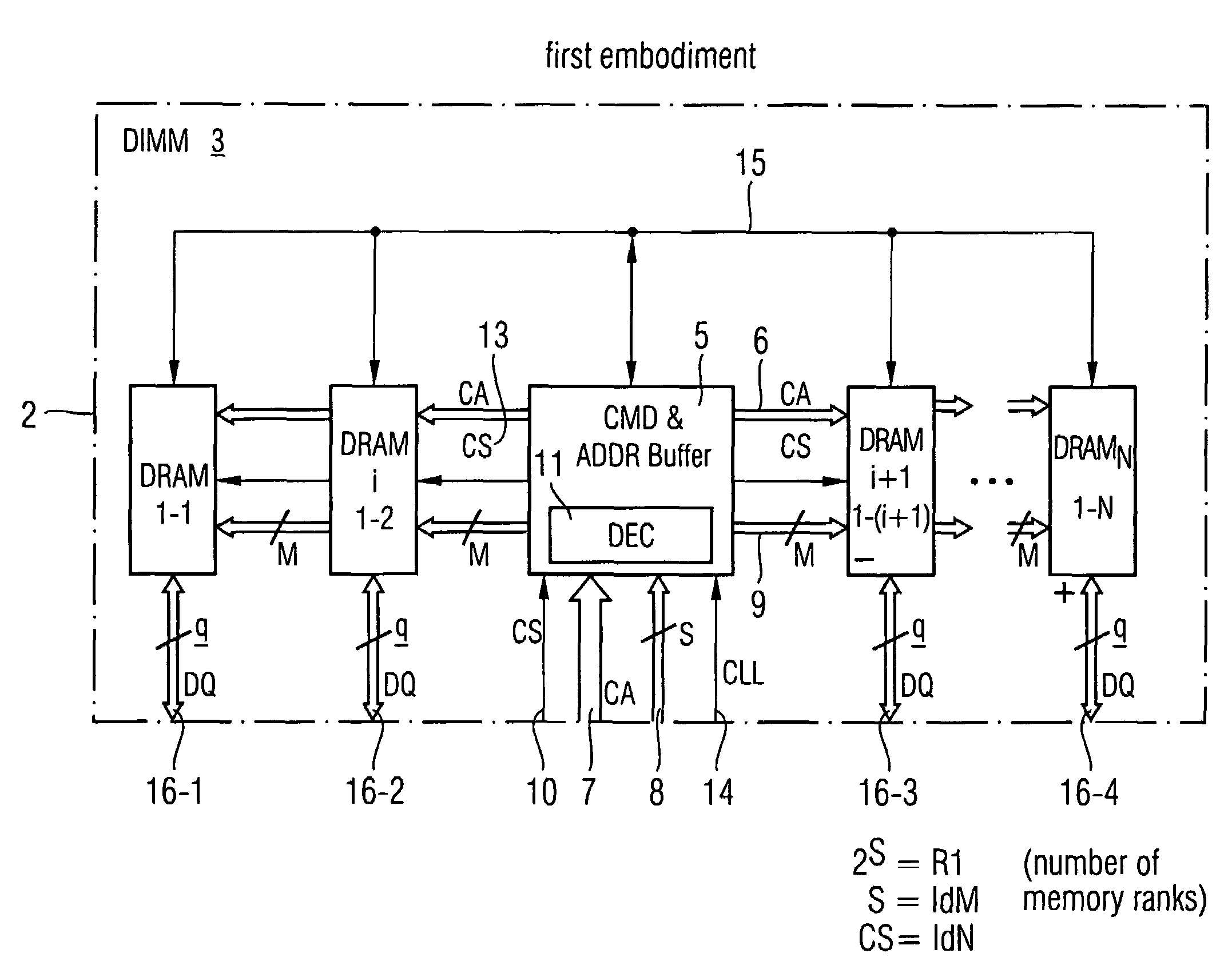
[0040]Referring to FIG. 4 it shows a dual inline memory module according to the present invention. On the dual inline memory module 3 a predetermined number M of DRAM memory chips 1 are mounted on a printed circuit board 2 of the dual inline memory module 3. The DRAM memory chips 1 are stacked DRAM chips. Each DRAM chip 1 comprises a predetermined number M of stacked DRAM memory dies 4-i. Each memory die within the DRAM chip 1 is selectable by a corresponding memory rank selection signal. DRAM memory dies 4-i include each an array of memory cells which are addressable by address lines.

[0041]The dual inline memory module 3 comprises at least one central command and address buffer chip 5 which is located in the middle of the printed circuit board 2 of the dual inline memory module 3. The command and address buffer chip 5 is connected via a command and address bus 6 to all DRAM memory chips 1 on the dual inline memory module 3. The command and address buffer 5 received command and addr...

second embodiment

[0053]FIG. 7 shows a cross section through a stacked DRAM chip 1 mounted on the dual inline memory module 3 as shown in FIG. 6. The stacked DRAM chip 1 as shown in FIG. 7 comprises in the shown embodiment four stacked DRAM memory dyes 4-0, 4-1, 4-2, 4-3. Each memory die 4-i is selectable by a corresponding memory rank signal r-i. The DRAM memory dies 4-i include each an array of memory cells which are addressable by address lines. A common internal address bus comprises a predetermined number of internal address lines 17-i provided for addressing the memory cells of the memory dies 4-i.

[0054]FIG. 7 further shows as an example an address pad A0 connected via a address line 17-i to all memory dies 4-i. All address lines of the internal address bus are connected in parallel to all four DRAM memory dies of the stacked DRAM memory chip 1. The memory dies 4-i are clocked by a clock signal CLK applied to all memory dies 4-i via an internal clock line 18-i. The memory dies 4-i each are co...


PUM


Abstract

The invention refers to a Memory Rank Decoder for a Multi-Rank Dual Inline Memory Module (DIMM) having a predetermined number of DRAM memory chips mounted on a printer circuit board (PCB), wherein each DRAM memory chip comprises a predetermined number of stacked DRAM memory dies which are selectable by a memory rank selection signal (r), wherein the memory rank decoder generates the memory rank selection signal (r) in response to external selection signals applied to the dual inline module (DIMM).

Description

TECHNICAL FIELD[0001]The invention relates in general to a Memory Rank Decoder for a Multi-Rank Dual Inline Memory Module (DIMM) and in particular to a Memory Rank Decoder for a registered Dual Inline Memory Module (DIMM).BACKGROUND ART[0002]Memory modules are provided for increasing the memory capacity of a computer system. Originally single inline memory modules (SIMM) were used in personal computers to increase the memory size. A single inline memory module comprises DRAM chips on its printed circuit board (PCB) only on one side. The contacts for connecting the printed circuit board of the single inline memory module (SIMM) are redundant on both sides of the module. A first variant of SIMMs has thirty pins and provides 8 bits of data (9 bits in parity versions). A second variant of SIMMs which are called PS / 2 comprise 72 pins and provide 32 bits of data (36 bits in parity versions).[0003]Due to the different data bus width of the memory module in some processors, sometimes severa...

Claims


Application Information

Patent Timeline
IPC IPC(8): G06F12/00G11C8/06G11C8/12
CPCG11C5/04G11C8/12
Inventor RAGHURAM, SIVA
Owner POLARIS INNOVATIONS
Why Eureka
Try Eureka