
Semiconductor package having optical receptacles and light transmissive/opaque portions and method of making same

a technology of semiconductors and semiconductors, applied in the field of semiconductor packages, can solve the problems of not being suitable for many applications, the overall size of the resultant package, and the amount of space required to accommodate separate optical and electronic packages, so as to avoid damage to internal electrical leads, less cost, and high injection pressure and temperature

Inactive Publication Date: 2007-09-11
STANDRD MICROSYSTEMS CORPORATION
View PDF13 Cites 31 Cited by
  • Summary
  • Abstract
  • Description
  • Claims
  • Application Information

AI Technical Summary

Benefits of technology

"The patent describes a semiconductor package that includes a fiber-based optoelectronic device. The package is designed to have both the receptacles and the optical device in the same process, which simplifies the manufacturing process. The package also includes an optically transmissive material and an optically opaque material, which helps to secure the optical device in place and align the optical fiber with the device. The package can be made using a low-pressure, low-temperature molding process. The technical effects of this patent include improved manufacturing efficiency and more precise optical alignment."

Problems solved by technology

Though many high-performance optoelectronic interconnects have been developed for use within the telecommunications industry, they are not typically suitable for many applications (e.g., consumer-electronics) because of packaging and driver requirements, space needs, heat-dissipation problems, or cost.
Unfortunately, a major disadvantage of separate package designs is the overall size of the resultant package.
In particular, the amount of space required to accommodate separate optical and electronic packages is significant.
However, the cost involved in making two separate packages is even more significant—especially so in the cost-conscious consumer electronics market.
Not only must each package be separately manufactured and maintained, but having two packages might require the optical package not maintain a power supply as would be the case in the electronic package.
If the circuitry within the electronic package is defective, the optical package absent a power supply cannot bypass operation of its associated, defective electronic circuitry.
Unfortunately, conventional single package designs suffer from several disadvantages.
For example, fabrication problems may exist with respect to mating the various parts of the packaged device (i.e., the housing, the package support member and the optical receptacles).
These processes require relatively high curing temperatures, and thus, often cause significant thermal expansion within package parts fabricated from thermally conductive materials (e.g., ceramic substrates, metal lead frames, metal housings, etc.).
As such, misalignment between an optical receptacle (and thus, an optical fiber) and an optical device may result due to thermal expansion and contraction of the various parts during the high temperature curing / adhesion process and subsequent cooling process.
Unfortunately, active alignment is often time consuming, inefficient and unacceptably expensive for use in manufacturing computer interconnects.
For example, an unnecessary number of manufacturing steps is required to separately fabricate and assemble the various parts of the packaged device; these additional steps tend to increase manufacturing costs.

Method used


Image

  • Semiconductor package having optical receptacles and light transmissive/opaque portions and method of making same
  • Semiconductor package having optical receptacles and light transmissive/opaque portions and method of making same
  • Semiconductor package having optical receptacles and light transmissive/opaque portions and method of making same

Examples


Embodiment Construction

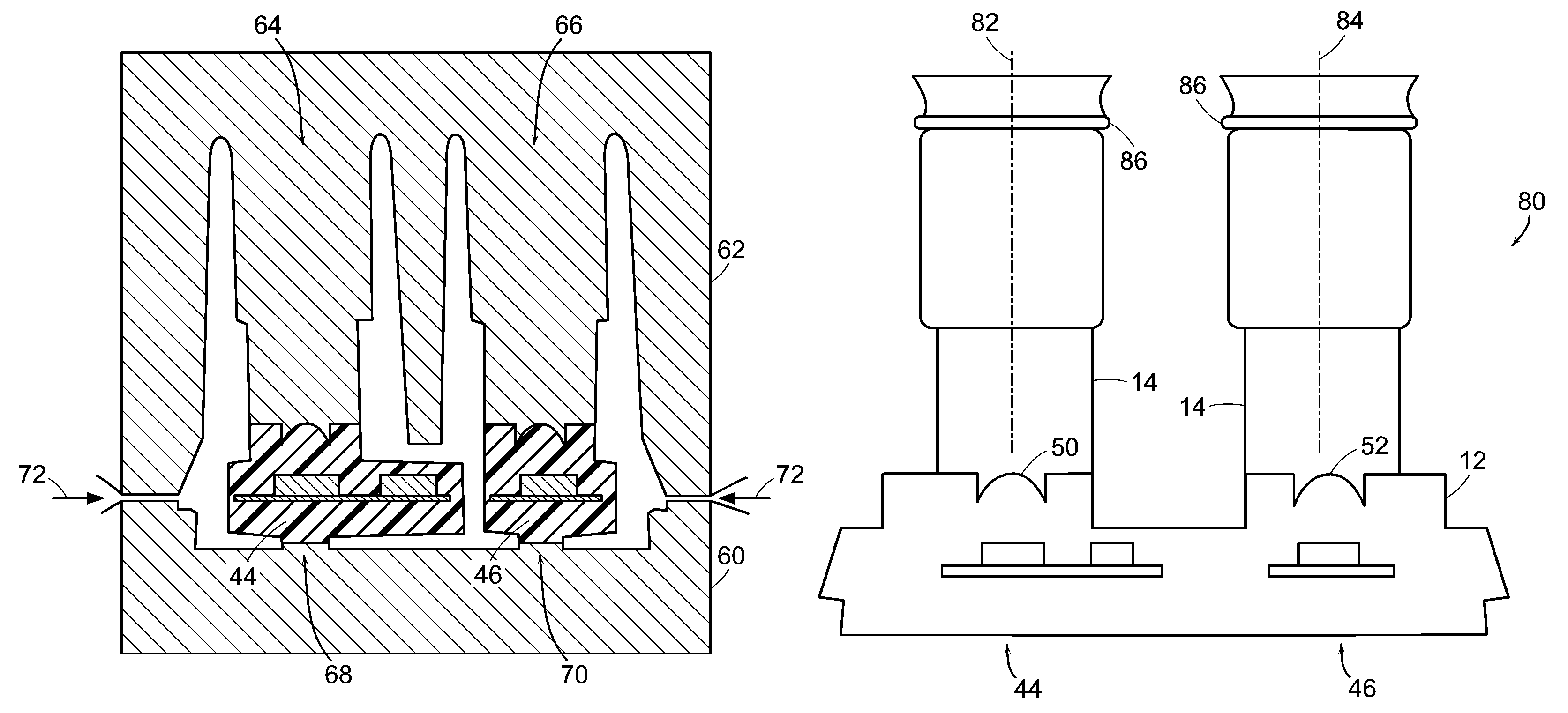
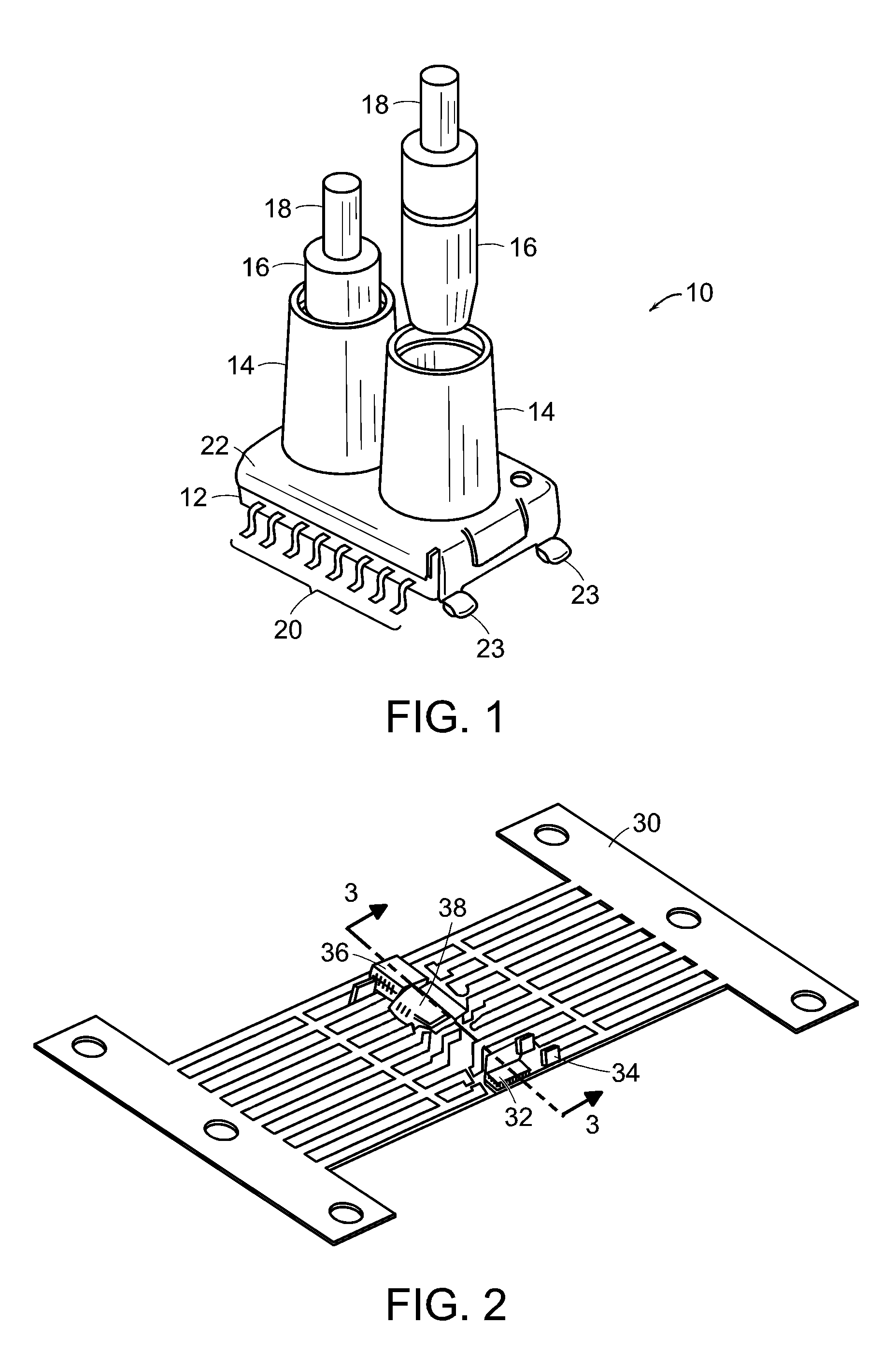
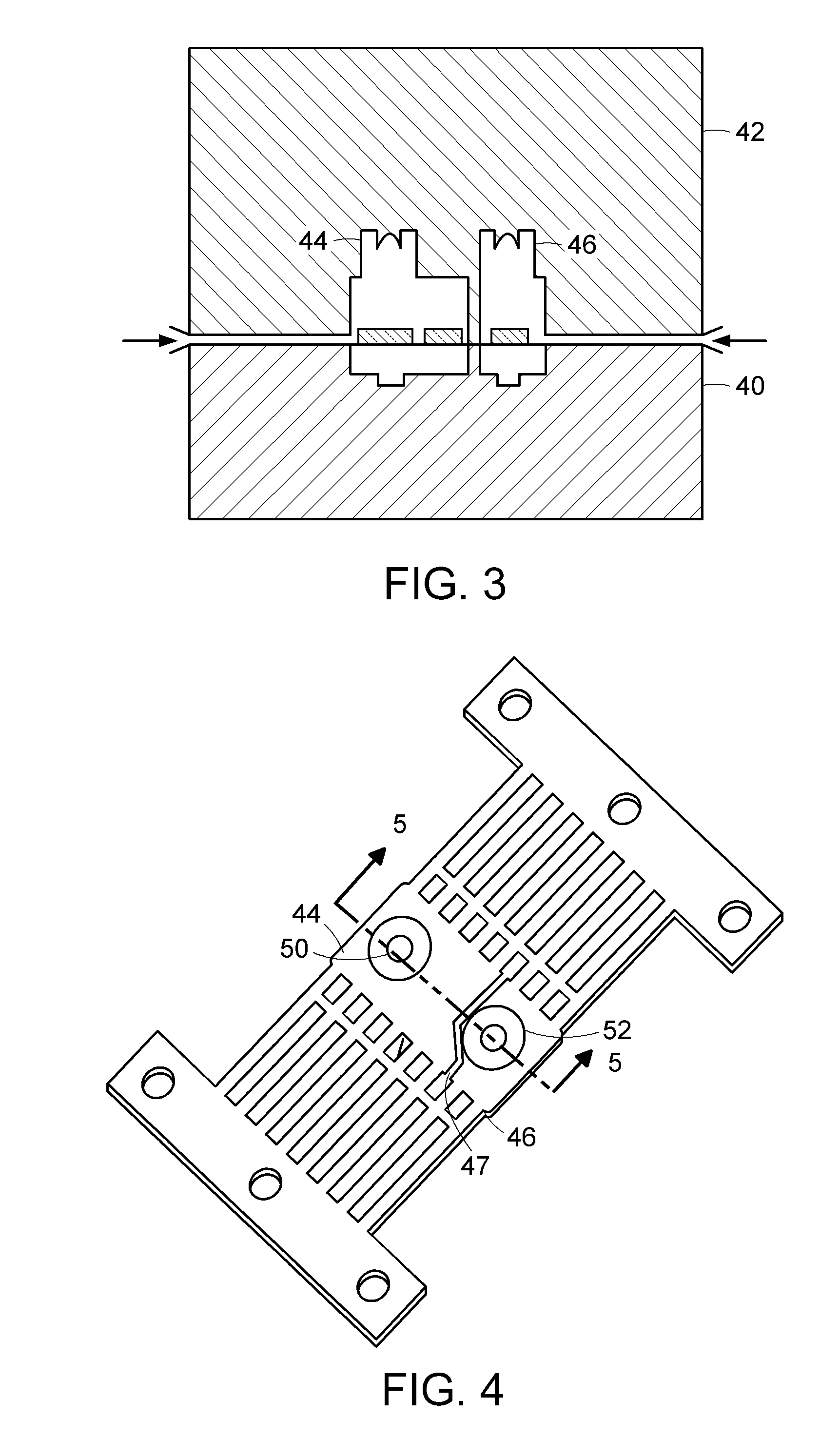
[0039]Optoelectronic interconnects may be fabricated to provide emission, detection, modulation and / or amplification of light. In most cases, however, optoelectronic interconnects include an optical source (i.e., an “optoelectronic transmitter” or an “emitter”) and / or an optical detector (i.e., an “optoelectronic receiver”), each of which is coupled to its own electronic support circuitry. In general, optoelectronic transmitters convert electrons into photons, which may then be transmitted across an optical transmission media, such as free-space, an optical fiber or waveguide. Optoelectronic receivers, on the other hand, convert photons received from the optical transmission media back into electrons.

[0040]The optical transmission media chosen for a given application is typically based on properties of the transmission path, such as path length, direction and clarity. For example, an optical signal may be transmitted through free-space when direct chip-to-chip, chip-to-board or boar...


PUM


Abstract

A semiconductor package and method for forming the same is disclosed herein. The semiconductor package includes a package support member, a pair of optoelectronic devices spaced from each other and coupled to the package support member, and an optically transmissive portion for separately encapsulating the pair of optoelectronic devices. A pair of lenses is formed as a unibody structure with the optically transmissive portion. The semiconductor package also includes an optically opaque portion, which extends between and around the separately encapsulated devices to optically isolate encapsulated optical devices. The optically opaque portion also extends outward from portions of the encapsulated devices, thereby forming a pair of fiber optic receptacles as a unibody structure with the optically opaque portion. By forming lensing elements and fiber optic receptacles in such a manner, the present method provides an easier and more accurate means by which to passively align optical conductors to underlying encapsulated optical devices.

Description

BACKGROUND OF THE INVENTION[0001]1. Field of the Invention[0002]This invention relates to semiconductor packages and, more particularly, to a semiconductor package comprising an optically transmissive portion, which separately encapsulates a pair of optoelectronic devices, and an optically opaque portion, which encapsulates the optically transmissive portion to optically isolate the pair of optoelectronic devices.[0003]2. Description of the Related Art[0004]The following descriptions and examples are not admitted to be prior art by virtue of their inclusion within this section.[0005]Optoelectronic devices are becoming increasingly common in automotive, consumer, medical, computer, and telecommunication applications due, in part, to the advantages of optical versus electrical signal transmission. For example, optoelectronic technologies have contributed significant advancements to the telecommunications industry by providing higher data rate and bandwidth capabilities than earlier wi...

Claims


Application Information

Patent Timeline
Patent Type & Authority Patents(United States)
IPC IPC(8): H01L31/12
CPCG02B6/423H01L31/0203H01L31/0232G02B6/4206H01L2224/48247H01L2924/1815H01L2924/3025H01L2224/48091H01L2924/00014H01L2924/00H01L31/02325
Inventor KNAPP, DAVID J.
Owner STANDRD MICROSYSTEMS CORPORATION
Features
  • Generate Ideas
  • Intellectual Property
  • Life Sciences
  • Materials
  • Tech Scout
  • Unparalleled Data Quality
  • Higher Quality Content
  • 60% Fewer Hallucinations
Learn More