Apparatus and method for customized burn-in of cores on a multicore microprocessor integrated circuit chip

a multi-core microprocessor integrated circuit and burn-in method technology, applied in the direction of electrical testing, measurement devices, instruments, etc., can solve the problems of continuous increase, wearout period, and the greatest failure rate of integrated circuit devices at the beginning and end of the average life cycle, so as to reduce the cost of the chip, improve burn-in yield, and achieve uniform power and performance

Inactive Publication Date: 2007-09-11
GOOGLE LLC
View PDF8 Cites 21 Cited by
  • Summary
  • Abstract
  • Description
  • Claims
  • Application Information

AI Technical Summary

Benefits of technology

[0014]The illustrative embodiments provide an apparatus and method for providing a multi-core integrated circuit chip that reduces the cost of the chip while optimizing performance of the cores for use with a single voltage plane. The apparatus and method of the illustrative embodiments make use of a dynamic burn-in technique that optimizes all of the cores on the chip to run at peak performance at a single voltage. Each core is burned-in with a customized burn-in voltage that provides uniform power and performance across the whole chip. This results in a higher burn-in yield and lower overall power in the integrated circuit chip.

Problems solved by technology

That is, it has been determined that the failure rate of integrated circuit devices is greatest at the beginning and end of the average life cycle of an integrated circuit chip.
The wear out period usually corresponds to failure induced by long-time waste and is continuously increased while time goes by.
In order to perform such accelerated testing, a testing environment that is harmful and dangerous to the integrated circuit chips is generated by testing equipment and the relationship between the failure rate and testing time is measured.
In order to generate the harmful testing environment, the chips are heated to an elevated temperature above which they are rated to function, and stressed by the application of voltage and current, also often in excess of what the chip is rated to withstand.
Thus, in the past, it was necessary to form the chips, individually handle the chips and test the chips individually, and only then were bad chips detected.
While this type of testing does work well, it requires a significant amount of processing of the wafer following the formation of the circuitry on and in the wafer before a determination is made that a chip is indeed bad.
This results in a higher burn-in yield and lower overall power in the integrated circuit chip.
Typically, NBTI threshold shifts are viewed as a reliability problem in modern integrated circuit devices.
Furthermore, applying the dynamic burn-in operation may comprise applying a burn-in voltage to the transistor gates of the at least one core in the to thereby shift a voltage bias of the transistor gates to cause the transistor gates to operate at different voltages via negative bias temperature instability (NBTI) affects.

Method used


Image

  • Apparatus and method for customized burn-in of cores on a multicore microprocessor integrated circuit chip
  • Apparatus and method for customized burn-in of cores on a multicore microprocessor integrated circuit chip
  • Apparatus and method for customized burn-in of cores on a multicore microprocessor integrated circuit chip

Examples


Embodiment Construction

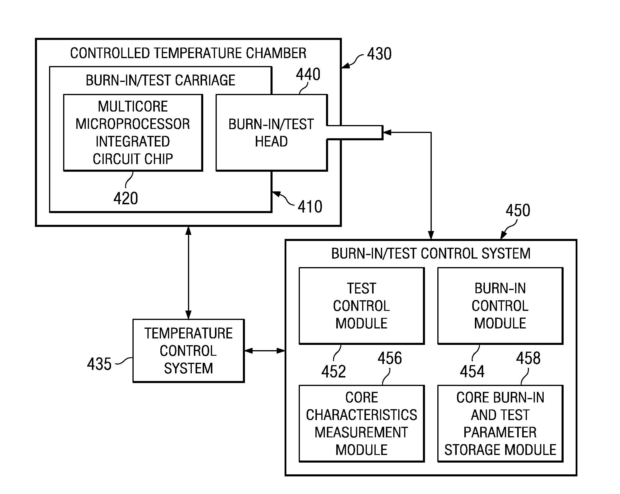
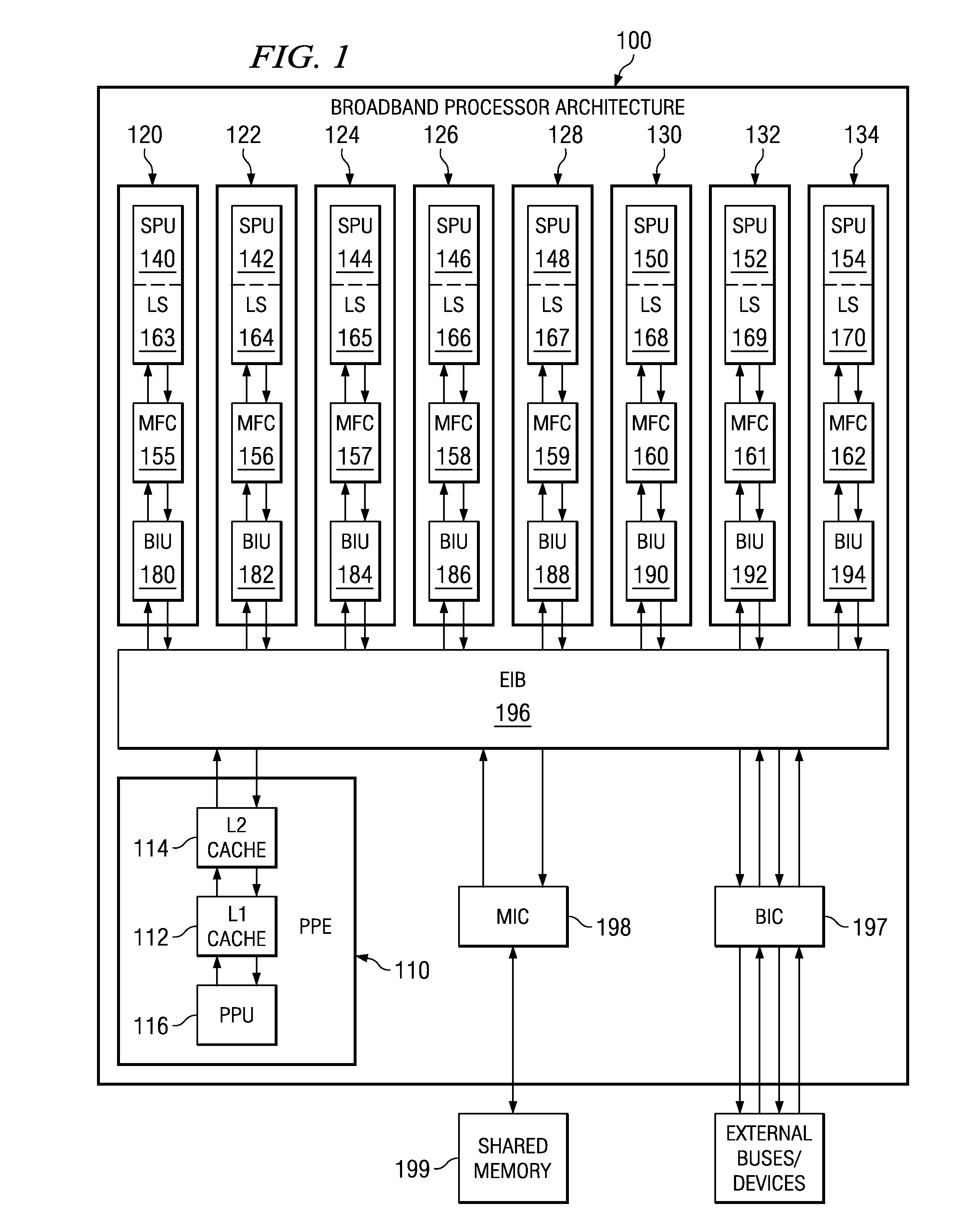
[0033]The illustrative embodiments provide an apparatus and method for performing customized burn-in of cores in a multicore integrated circuit chip. The mechanisms of the illustrative embodiments may be applied to any multicore integrated circuit chip and are not limited to any particular configuration. For purposes of illustration, however, the following description of the illustrative embodiments will make reference to the Cell Broadband Engine (CBE), also known as the Broadband Processor Architecture, available from International Business Machines, Inc., as an example of a multicore microprocessor that may be provided on an integrated circuit chip and stressed using the customized burn-in process of the illustrative embodiments. While the CBE will be used for illustrative purposes, this is not to state or imply any limitation with regard to the types of multicore integrated circuit chips in which the illustrative embodiments may be implemented or with which the illustrative embo...


PUM


Abstract

An apparatus and method for providing a multi-core integrated circuit chip that reduces the cost of the package and board while optimizing performance of the cores for use with a single voltage plane. The apparatus and method of the illustrative embodiments make use of a dynamic burn-in technique that optimizes all of the cores on the chip to run at peak performance at a single voltage. Each core is burned-in with a customized burn-in voltage that provides uniform power and performance across the whole chip. This results in a higher burn-in yield and lower overall power in the integrated circuit chip. The optimization of the cores to run at peak performance at a single voltage is achieved through use of the negative bias temperature instability affects on the cores imparted by the burn-in voltages applied.

Description

BACKGROUND[0001]1. Technical Field[0002]The present application relates generally to an apparatus and method for providing an improved integrated circuit device. More specifically, the present application is directed to an apparatus and method for customized burn-in of cores on a multicore microprocessor integrated circuit chip.[0003]2. Description of Related Art[0004]In the manufacture and testing of integrated circuit chips, a common technique is to form a wafer of semi-conductive material, such as silicon, and to form in and on the wafer the necessary circuitry for a multiplicity of integrated circuit chips. The wafer is formed with all of the circuitry necessary for the functioning of each of the chips, including I / O contacts for connecting to I / O signals, power and ground. The contacts may be for either wire bond connections or compressive bonding connections or for controlled collapse chip connect (C4) bonds which utilizes solder balls for flip chip bonding.[0005]Whatever type...

Claims


Application Information

Patent Timeline
Patent Type & Authority Patents(United States)
IPC IPC(8): G01R31/02
CPCG01R31/2855
Inventor AUDET, JEANCAPPS, JR., LOUIS B.DAVES, GLENN G.FERRIS, JOANNEHARIDASS, ANANDNEWHART, RONALD E.SHAPIRO, MICHAEL J.
Owner GOOGLE LLC
Why Eureka
Try Eureka