Semiconductor device for driving a load

a technology of a semiconductor device and a load, which is applied in the direction of semiconductor devices, oscillator generators, pulse techniques, etc., can solve the problems of increasing the risk of thermal breakdown of mosfet b>3/b>, weakening the competitiveness of the market, etc., to prevent thermal breakdown reduce the heat produced in the first switching element, and increase the size of the first switching element

Inactive Publication Date: 2007-09-11
DENSO CORP
View PDF6 Cites 14 Cited by
  • Summary
  • Abstract
  • Description
  • Claims
  • Application Information

AI Technical Summary

Benefits of technology

[0007]In view of the above problem, it is an object of the present invention to provide a semiconductor device for driving a load, the device having a semiconductor switching element, adequate thermal margin of which can be provided without increasing size of the switching element.
[0010]The power supply voltage is divided between the first switching element and the second switching element. Heat produced in the first switching element can be reduced. Thermal margin of the first switching element increases accordingly. Therefore, there is no need to increase the size of the first switching element to prevent thermal breakdown of the first switching element. A cost competitiveness can be enhanced.

Problems solved by technology

In other words, the risk of thermal breakdown of the MOSFET 3 is increased.
Therefore, it is required to increase the size of the MOSFET 3 to prevent thermal breakdown of the MOSFET 3 and cost competitiveness is weakened.

Method used


Image

  • Semiconductor device for driving a load
  • Semiconductor device for driving a load
  • Semiconductor device for driving a load

Examples


Embodiment Construction

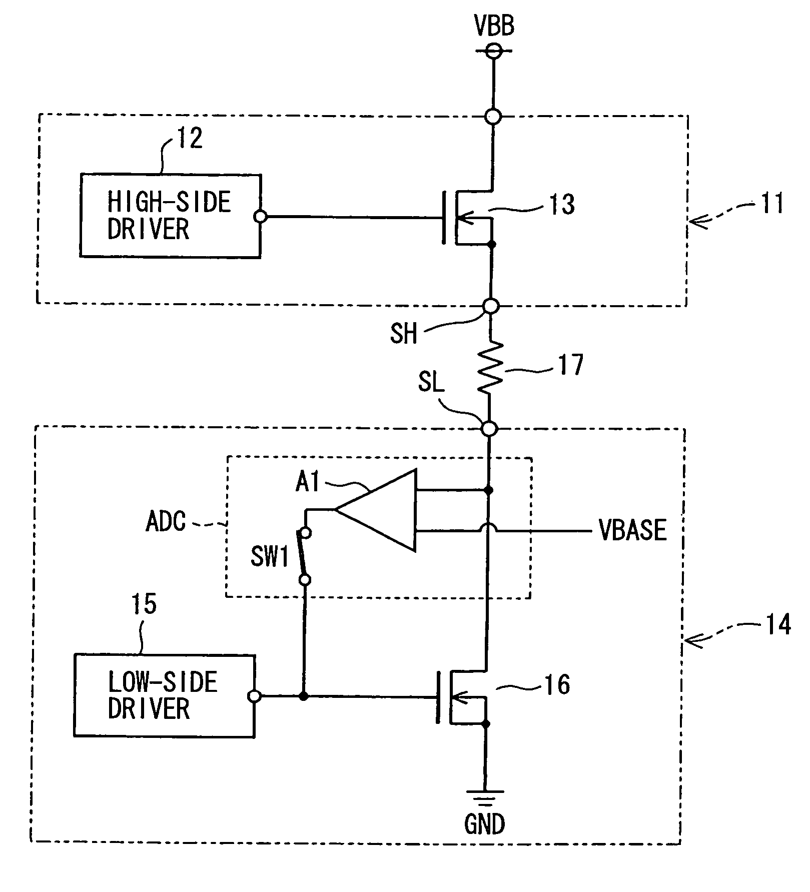
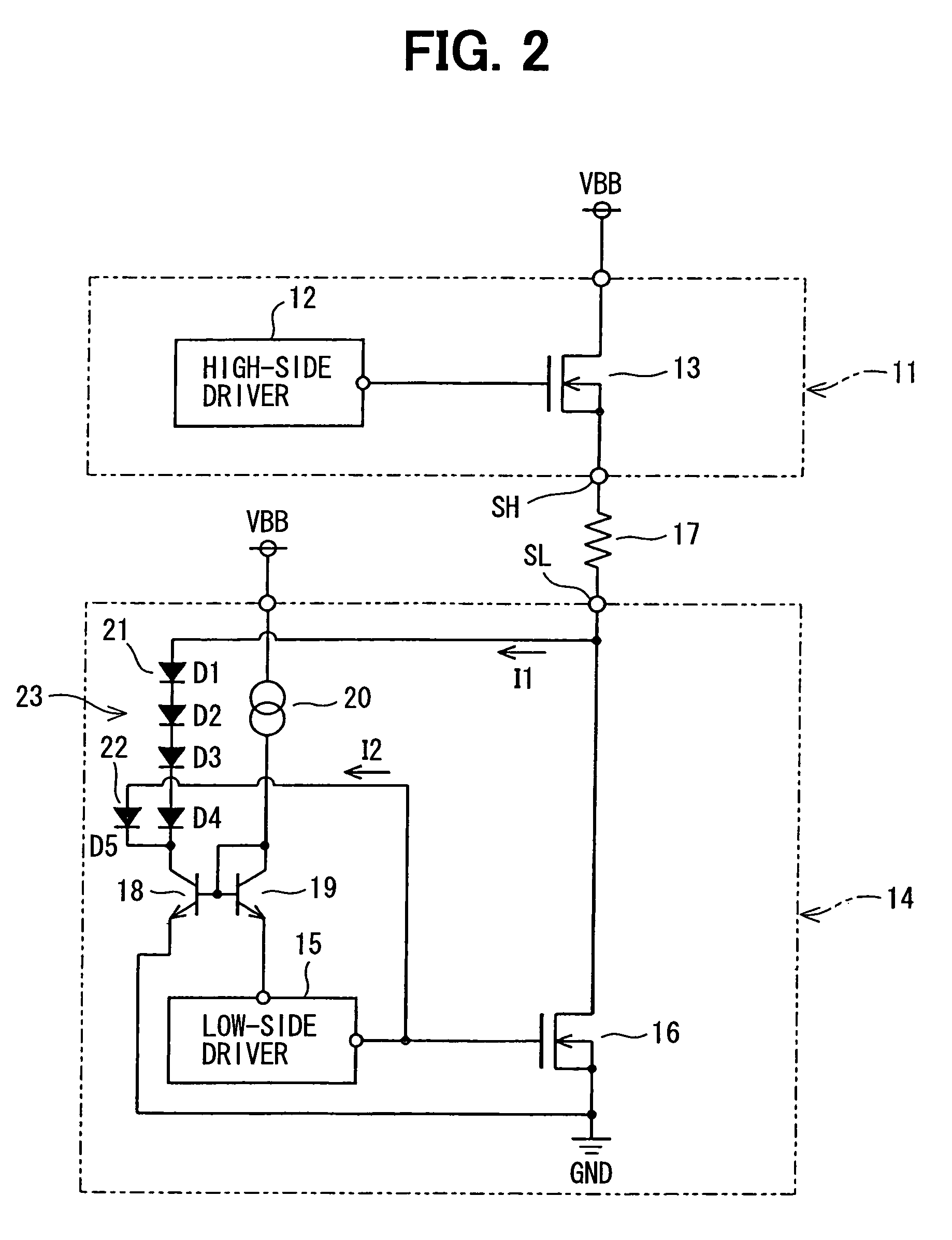
[0015]Reference is made first to FIG. 1, which shows a semiconductor device used as a driver circuit in an airbag ECU. The driver circuit has a high-side circuit 11 and a low-side circuit 14.

[0016]The high side circuit 11 includes a high-side driver 12 fed from a charge-pump type voltage step-up circuit (not shown) and an n-channel LDMOS (Laterally Diffused MOSFET) 13 provided as the first semiconductor switching element. A voltage of a gate terminal (a control terminal) of the LDMOS 13 is controlled by the high-side driver 12. A drain terminal and a source terminal of the LDMOS 13 are connected to a power supply terminal VBB and an output terminal SH, respectively. The low-side circuit 14 includes a low-side driver 15 and an n-channel LDMOS 16 provided as the second semiconductor switching element. The low-side driver 15 controls a voltage of a gate terminal of the LDMOS 16 and switches on and off the LDMOS 16. A drain terminal and a source terminal of the LDMOS 16 are connected to...


PUM


Abstract

A semiconductor device for driving a load includes a first semiconductor switching element interposed between a power supply terminal and a load, a second semiconductor switching element interposed between the load and a ground terminal, a high-side driver, a low-side driver, and a voltage regulator. The voltage regulator reduces a voltage applied to a control terminal of the second switching element, when a voltage of a load terminal of the second switching element is lower than a predetermined voltage. Then, a voltage applied between the load terminal and the ground terminal of the second switching element increases, and accordingly a voltage applied between the power supply terminal and the load terminal of the first switching element decreases.

Description

CROSS REFERENCE TO RELATED APPLICATION[0001]This application is based on Japanese Patent Application No. 2004-310865 filed on Oct. 26, 2004, the disclosures of which are incorporated herein by reference.FIELD OF THE INVENTION[0002]The present invention relates to a semiconductor device for driving a load, the device including a first semiconductor switching element controlled by a high-side driver and a second semiconductor switching element controlled by a low-side driver.BACKGROUND OF THE INVENTION[0003]A squib driver integrated circuit (IC) for driving an airbag squib is disclosed in a data sheet of a squib driver TPD2004F of Toshiba Semiconductor Company published on Sep. 11, 1998.[0004]FIG. 3 is a simplified circuit diagram of the squib driver IC. A high-side circuit 1 includes an n-channel metal oxide semiconductor field effect transistor (MOSFET) 3 and a high-side driver 2, which is a charge-pump type. The high-side driver 2 controls a gate voltage of the MOSFET 3. A drain an...

Claims


Application Information

Patent Timeline
Patent Type & Authority Patents(United States)
IPC IPC(8): H03B1/00
CPCH03K17/04206H03K17/0822
Inventor OTA, KINGOOKUDA, SHOICHIABE, HIROFUMI
Owner DENSO CORP
Why Eureka
Try Eureka