Optical element and optical scanning device using the same

a scanning device and optical element technology, applied in the direction of printing, instruments, inking apparatus, etc., can solve the problems of difficult control of volume ratio or aspect ratio between a base material, difficult to inexpensively (simply) manufacture sws, and limit the reduction of cost, so as to achieve uniform anti-reflection characteristics

Inactive Publication Date: 2007-09-11
CANON KK
View PDF31 Cites 45 Cited by
  • Summary
  • Abstract
  • Description
  • Claims
  • Application Information

AI Technical Summary

Benefits of technology

[0017]It is an object of the present invention to provide an optical element which is capable of obtaining uniform anti reflection characteristics over the whole optical surface of the optical element having a finite curvature, a method of manufacturing the optical element, and an optical scanning device using the optical element.
[0032]According to the present invention, it is possible to realize an optical element which is capable of obtaining uniform anti reflection characteristics over the whole optical surface by providing a plurality of convex optical members having an anti reflection function on a surface of the optical element having a finite curvature.

Problems solved by technology

Even with any of those film deposition means taken, the film deposition must be carried out after an optical element base is processed, so the optical element is difficult to manufacture, and thus there is a limitation in the reduction of cost.
With this method, there is an advantage that a precisely designed SWS can be formed, but this method involves a problem in that there are many limitations to a case where the SWS is formed over a large area on a curved surface, and thus the SWS is very difficult to inexpensively (simply) manufacture.
However, since the minute particles are continuously and uniformly arranged to construct the SWS, there has been a problem in that it is difficult to control a volume ratio or aspect ratio between a base material and an atmosphere, which determines reflection characteristics, and thus it is difficult to obtain an ideal anti reflection effect.
However, since an anti reflection film is difficult to be formed on a surface of a plastic lens from the technical and cost reasons, the anti reflection film may be omitted.
As a result, the surface reflection may be generated from each optical surface to cause nonconformity.

Method used


Image

  • Optical element and optical scanning device using the same
  • Optical element and optical scanning device using the same
  • Optical element and optical scanning device using the same

Examples


embodiment 1

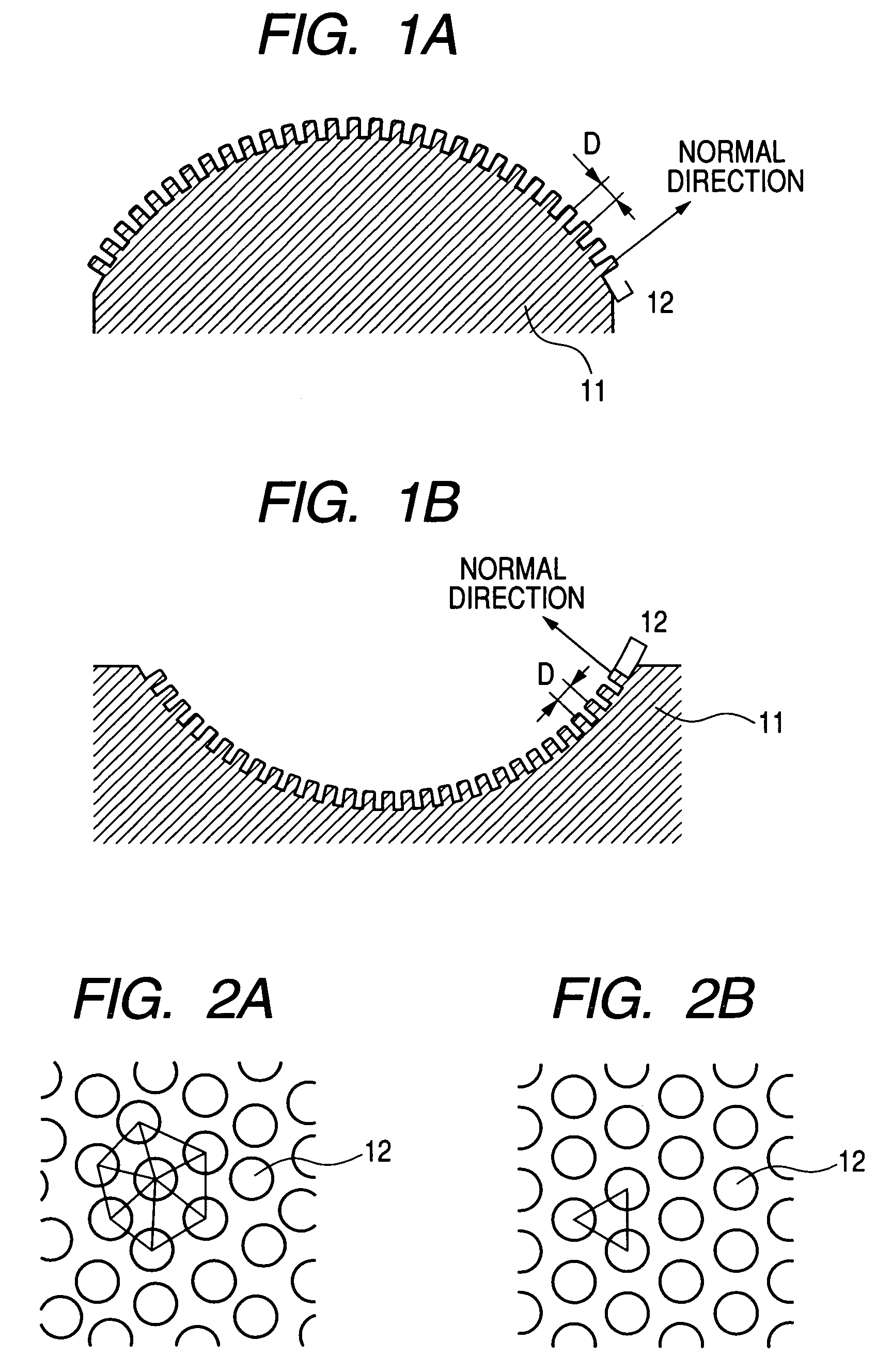
[0045]FIGS. 1A and 1B are views each schematically showing a cross section of an optical element according to Embodiment 1 of the present invention. FIG. 1A shows a case where a base shape of an optical surface has a convex surface, and FIG. 1B shows a case where a base shape of an optical surface has a concave surface.

[0046]In FIGS. 1A and 1B, reference numeral 11 designates an optical element (optical member) having a finite curvature (a finite curvature except for infinity). A base shape of an optical surface of the optical element 11 is formed so as to have a convex surface or a concave surface. The optical surface of the optical element 11 in Embodiment 1 has a refracting surface for example.

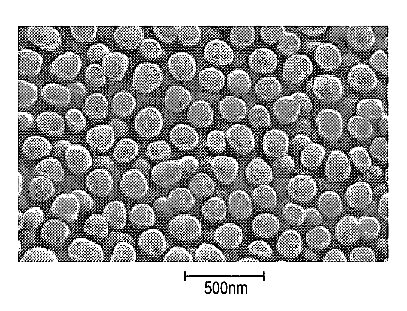
[0047]FIG. 3A is a schematic view schematically showing a cross section of a plurality of optical pieces according to Embodiment 1 of the present invention.

[0048]Reference numeral 12 designates a fine optical piece (convex portion) having an anti reflection function. A plurality of optical ...

embodiment 2

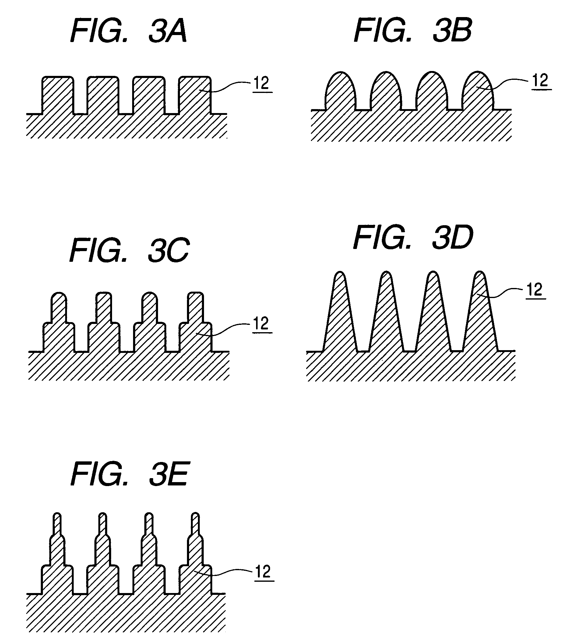
[0068]FIGS. 3B, 3C, 3D and 3E are schematic views each schematically showing a cross section of a plurality of optical pieces according to Embodiment 2 of the present invention.

[0069]Embodiment 2 is different from Embodiment 1 in that an optical piece is formed in shape of becoming radially slenderer (toward a head portion) as distant from the surface of the optical element 11 having the finite curvature. Other constructions and optical operations are nearly the same as those in Embodiment 1, and thus the same effects as those in Embodiment 1 are obtained.

[0070]FIG. 3B shows a situation in which a radial thickness of the optical piece 12 becomes slenderer toward a head portion, FIG. 3C shows a situation in which a radial thickness of the optical piece 12 becomes slenderer in shape having one step toward a head portion, FIG. 3D shows a situation in which a radial thickness of the optical piece 12 becomes slenderer in a tapered manner toward a head portion, and FIG. 3E shows a situati...


PUM


Abstract

To obtain an optical element capable of obtaining uniform anti reflection characteristics over the whole optical surface having a finite curvature of the optical element, a plurality of convex optical pieces having an anti reflection function are provided on a surface having the finite curvature of the optical element independently along a normal direction of the surface having the finite curvature of the optical element.

Description

BACKGROUND OF THE INVENTION[0001]1. Field of the Invention[0002]The present invention relates to an optical element having a function of suppressing a quantity of light reflected by an interface in an incidence / emission surface for light, a method of manufacturing the optical element, and an optical apparatus using the optical element, and is suitable for an image pickup device such as a camera or a video camera, or an optical scanning device used in a liquid crystal projector or an electrophotographic apparatus (such as a digital copying machine or a laser beam printer).[0003]2. Related Background Art[0004]Generally, in an optical element in which a quantity of light reflected on a surface is required to be suppressed, a signal layer or a plurality of layers of optical films having refractive indices different from one another are laminated on a surface of the optical element by a thickness of several tens to several hundreds of nanometers to obtain desired reflection characteristi...

Claims


Application Information

Patent Timeline
Patent Type & Authority Patents(United States)
IPC IPC(8): G02B5/18B41J15/14B41J27/00G02B5/02G02B6/34G02B26/12
CPCG02B1/118G02B26/125G02B5/02
Inventor MATSUO, YASUHIROISHIBE, YOSHIHIROKIMURA, KAZUMINOMURA, KENTAROU
Owner CANON KK
Why Eureka
Try Eureka