Method and system for hard failure repairs in the field

a hard failure and repair technology, applied in the field of hard failure repair methods and systems, can solve the problems of increasing the number of devices and/or interconnections, affecting system reliability and repair, and reducing the system failure rate, so as to improve system reliability, reduce system failure rate, and improve system reliability. the effect of continuous monitoring

Inactive Publication Date: 2007-10-02
ALTERA CORP
View PDF25 Cites 35 Cited by
  • Summary
  • Abstract
  • Description
  • Claims
  • Application Information

AI Technical Summary

Benefits of technology

[0011]Many benefits are achieved by way of the present invention over conventional techniques. For example, certain embodiments of the present invention provide self-healing systems that can detect failures and repair such failures by themselves. Some embodiments of the present invention enables failure detection and repair in the field. For example, a failure is detected and repaired in the field. Certain embodiments of the present invention provide efficient and continuous monitoring of system reliability. For example, the monitoring is performed by tested systems without or with limited interaction with external systems. Some embodiments of the present invention provide repairs of hard failures. For example, the repairs are performed without or with limited interaction with external systems. As another example, the repairs are performed with a repair voltage less than or equal to an operation voltage used by the system under test. For example, the repair voltage equals about 3.3 volts. Certain embodiments of the present invention use polysilicon fuses in tested systems. For example, the tested systems implement FPGA architectures. Some embodiments of the present invention use redundancy in tested systems. Certain embodiments of the present invention use error correction codes implemented in tested systems. Some embodiments of the present invention improve system reliability. For example, test systems have a large number of transistors and / or interconnects. The transistors may have a feature size that has become smaller with each generation of integrated circuits. The interconnects may include numerous single vias. The decreasing size and the increasing number of devices and / or interconnects pose a significant challenge to system reliability and repair. In another example, copper interconnects may suffer from via pull back which is a time dependent phenomena. Some embodiments of the present invention can significantly reduce system failure rate, such as the failure rate for 109 device hours (FIT).

Problems solved by technology

The decreasing size and the increasing number of devices and / or interconnects pose a significant challenge to system reliability and repair.

Method used


Image

  • Method and system for hard failure repairs in the field
  • Method and system for hard failure repairs in the field
  • Method and system for hard failure repairs in the field

Examples


Embodiment Construction

[0021]The present invention relates generally to failure repairs for electronic systems. More specifically, the invention provides a method and system for repairing hard failures in the field. Merely by way of example, the invention has been applied to integrated circuits such as FPGAs, but it would be recognized that the invention has a much broader range of applicability.

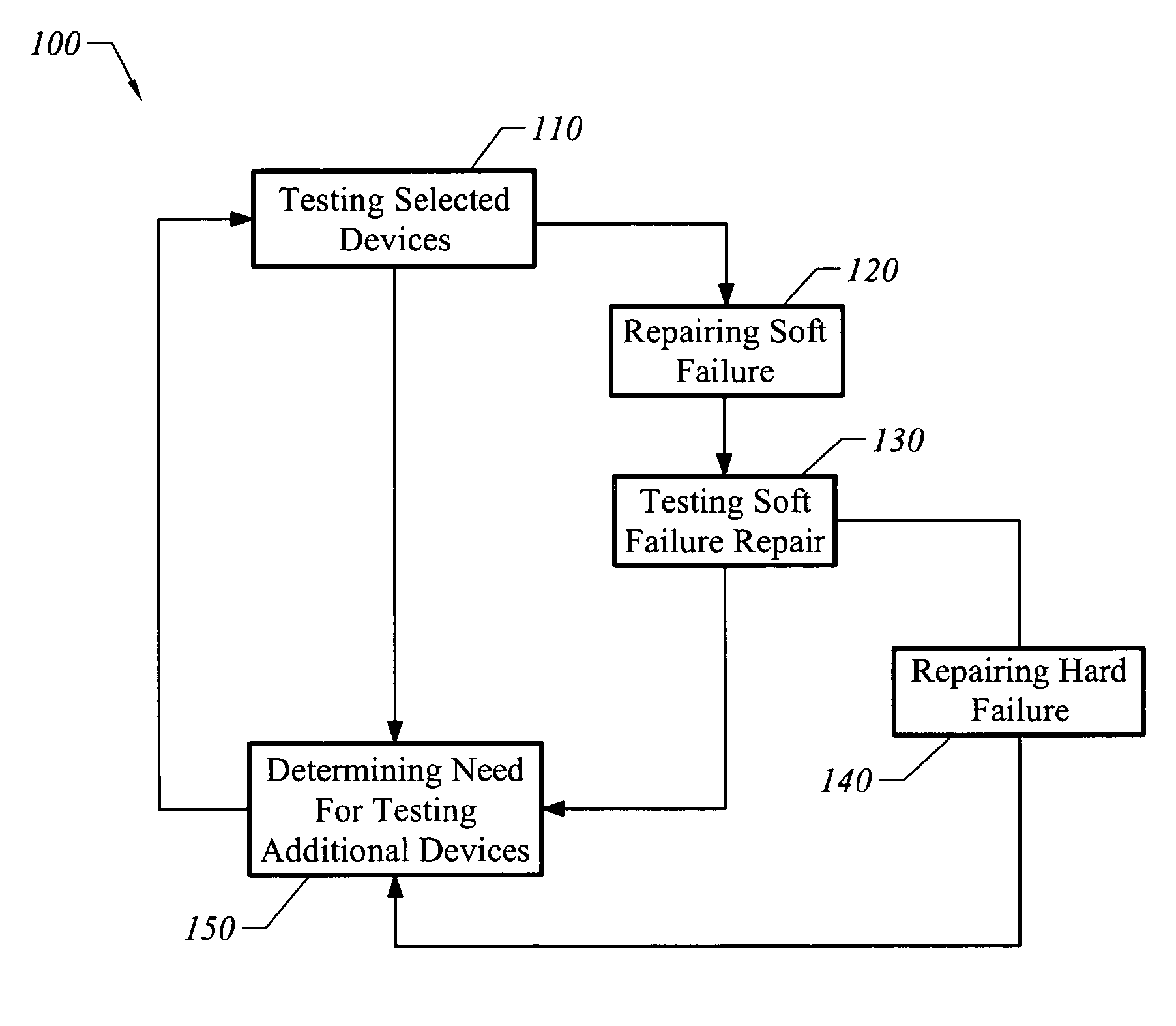
[0022]FIG. 1 is a simplified method for repairing failures according to an embodiment of the present invention. This diagram is merely an example, which should not unduly limit the scope of the claims herein. The method 100 includes process 110 for testing selected devices, process 120 for repairing soft failure, process 130 for testing soft failure repair, process 140 for repairing hard failure, and process 150 for determining need for testing additional devices. Although the above has been shown using a selected sequence of processes, there can be many alternatives, modifications, and variations. For example, so...


PUM


Abstract

A semiconductor system and method for repairing failures of a packaged integrated circuit system are provided. The method includes detecting a failure associated with a packaged integrated circuit system after the packaged integrated circuit system is packaged, and repairing the failure by activating a redundancy circuit in the packaged integrated circuit system and deactivating a defective circuit associated with the failure. The process for repairing the failure includes applying a repair voltage to a polysilicon fuse to change a conductivity state of the polysilicon fuse from a first state to a second state. In another embodiment, the polysilicon fuse is replaced by a metal fuse, an anti-fuse, or a non-volatile random access memory.

Description

CROSS-REFERENCES TO RELATED APPLICATIONS[0001]Not ApplicableSTATEMENT AS TO RIGHTS TO INVENTIONS MADE UNDER FEDERALLY SPONSORED RESEARCH OR DEVELOPMENT[0002]Not ApplicableREFERENCE TO A “SEQUENCE LISTING,” A TABLE, OR A COMPUTER PROGRAM LISTING APPENDIX SUBMITTED ON A COMPACT DISK[0003]Not ApplicableBACKGROUND OF THE INVENTION[0004]The present invention relates generally to failure repairs for electronic systems. More specifically, the invention provides a method and system for repairing hard failures in the field. Merely by way of example, the invention has been applied to integrated circuits such as field-programmable gate arrays (FPGAs), but it would be recognized that the invention has a much broader range of applicability.[0005]Integrated circuits (ICs) usually include millions of devices. The large number of devices has significantly improved circuit complexity. Additionally, the feature size of the smallest devices has been reduced in order to improve circuit density. High ci...

Claims


Application Information

Patent Timeline
Patent Type & Authority Patents(United States)
IPC IPC(8): G11C17/18
CPCG11C17/18G11C29/4401G11C29/42G11C17/14G11C2029/0409
Inventor RAHIM, IRFANMCELHENY, PETER J.CHANG, ERIC CHOONG-YIN
Owner ALTERA CORP
Why Eureka
Try Eureka