Sensor, scanner and portable information terminal each having liquid crystal display

a liquid crystal display and sensor technology, applied in the direction of optical radiation measurement, radiation controlled devices, instruments, etc., can solve the problems of low light utilization efficiency, slow reading speed or mechanical strength, weak signal, etc., and achieve the effect of high light utilization efficiency

Inactive Publication Date: 2007-10-09
SEMICON ENERGY LAB CO LTD
View PDF8 Cites 11 Cited by
  • Summary
  • Abstract
  • Description
  • Claims
  • Application Information

AI Technical Summary

Benefits of technology

[0037]It is an object of the present invention to resolve the above-described problem of the conventional technology. Further specifically, it is a problem of the present invention to provide a close contact type sensor having high light utilizing efficiency.
[0039]In a single pixel, by providing a large number of irradiation windows by reducing a size of a single irradiation window, regions of portions of a light receiving portion and an irradiation window at a vicinity of a boundary therebetween can be increased. Further, a region of an irradiation window remote from a light receiving portion and a region of a light receiving portion remote from an irradiation window are reduced. Therefore, the light utilizing efficiency is promoted. As a result, a magnitude of an output signal from a pixel of a sensor is increased. Therefore, image quality read by a sensor is promoted. Further, power consumption of a light source can be reduced since the light utilizing efficiency is high.
[0040]Next, when light is irradiated from a side opposed to a reading object to an irradiation window, light is made to irradiate to only an irradiation window portion as much as possible and light is prevented from irradiating to a sensor circuit portion as less as possible. Or, the irradiation window portion is made to arrange at a region irradiated with light. As a result, light which does not reach the reading object, that is, wasteful light is reduced and the light utilizing efficiency is promoted. Further, power consumption of a light source can be reduced since the light utilizing efficiency is high.

Problems solved by technology

Therefore, the apparatus is large-sized, reading speed is retarded or mechanical strength is weakened.
Therefore, the light utilizing efficiency is not high, as a result, the signal is also weak.
Further, since light irradiated also to portions other than the irradiation window 307, the light utilizing efficiency is not high and more power consumption is needed.
Further, as the reflection angle is increased, the intensity of the reflected light is weakened.
That is, the reflected light is wasted.
That is, when single pieces of the large light receiving portion 306 and the large irradiation window 307 are arranged, the light utilizing efficiency is very poor.
As a result, a characteristic of the sensor such as sensitivity is deteriorated.
That is, light irradiated to the sensor circuit portion is totally wasted.
As a result, the light utilizing efficiency is lowered.
Therefore, an increase in power consumption is caused for irradiating stronger light to the reading object 304.

Method used


Image

  • Sensor, scanner and portable information terminal each having liquid crystal display
  • Sensor, scanner and portable information terminal each having liquid crystal display
  • Sensor, scanner and portable information terminal each having liquid crystal display

Examples


embodiment 1

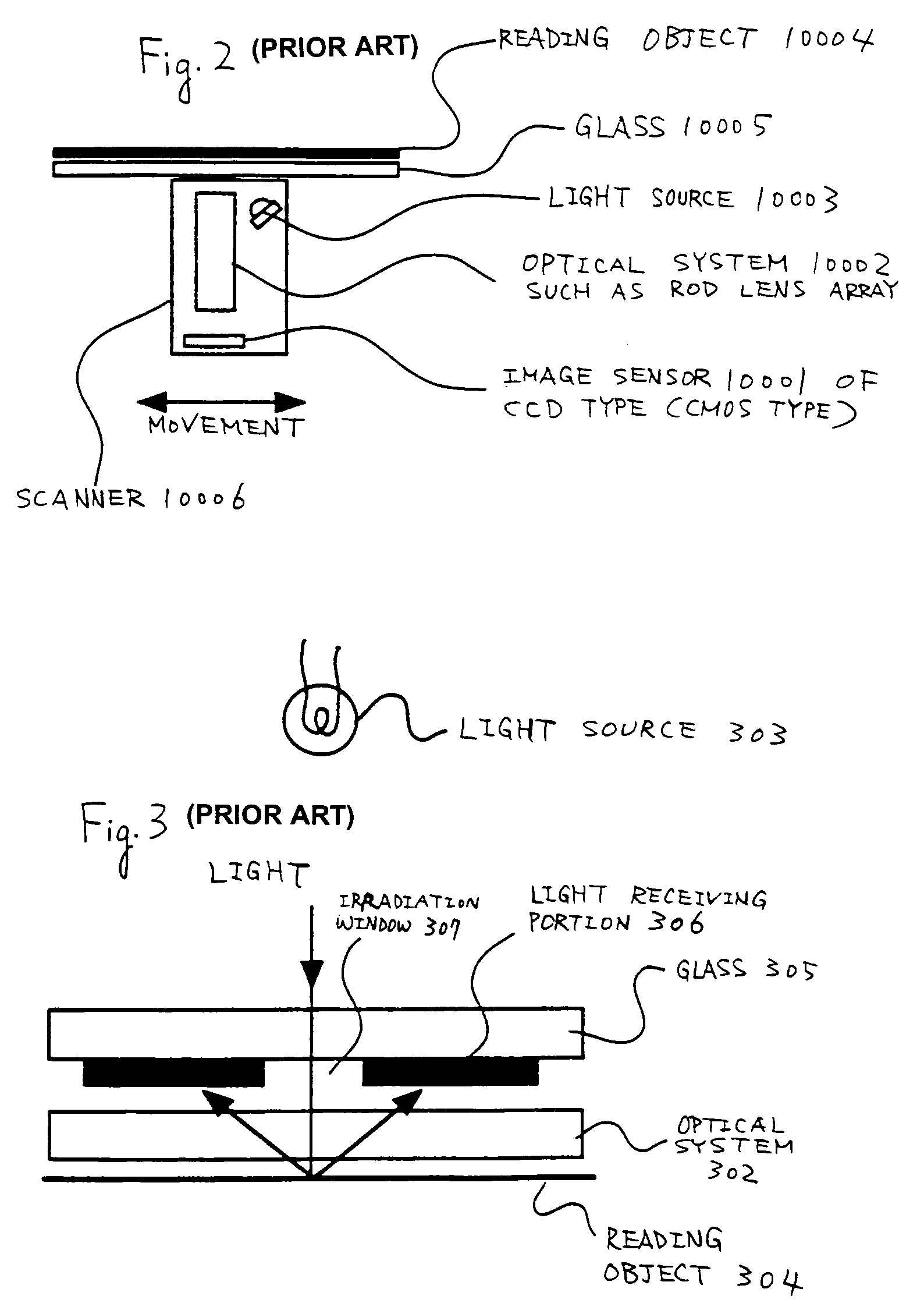
[0106]FIG. 8 shows a view viewing, from above, a case in which a plurality of irradiation windows 807 are provided in a single pixel. FIG. 9 shows a sectional view of FIG. 8 taken along a section line 801. The number of the irradiation windows 807 may be any number so far as the number is a plural number. Glass 805 is formed with light receiving portions 806, circuit portions and the irradiation windows 807. The irradiation window 807 is made to be transparent for transmitting light. According to the light receiving portion 806, a light shielding film is frequently formed between the light receiving portion 806 and the glass 806 such that influence is not effected thereon even when light is incident thereon from a side opposed to a reading object 804. Further, the light receiving portion 806 and the circuit portion may be arranged to overlap.

[0107]Further, although in FIG. 9, for simplicity, only the light receiving portions 806 and the irradiation windows 807 are illustrated on the...

embodiment 2

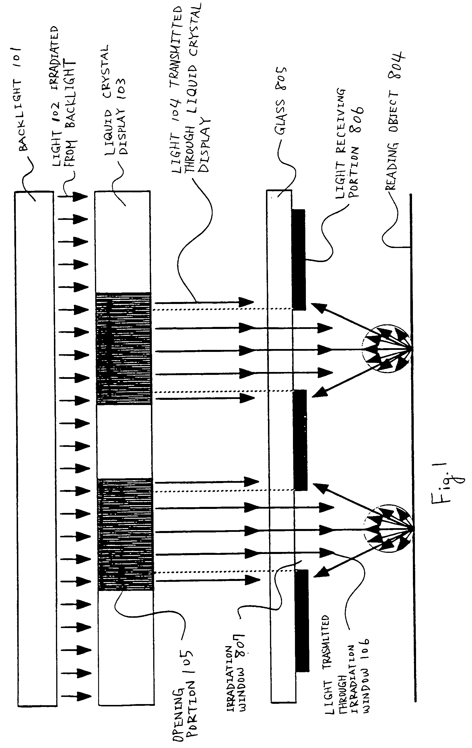
[0111]FIG. 1 shows a sectional view of a close contact type sensor when a liquid crystal display and a backlight are used as a light source for a sensor. A backlight 101 is provided at the topmost position, a liquid crystal display 103 is provided therebelow, the light receiving portions 806 and the irradiation windows 807 are provided therebelow and the reading object 804 are provided therebelow.

[0112]The glass 805 is formed with the light receiving portions 806, circuit portions and the irradiation windows 807. The irradiation window 807 is made to be transparent for transmitting light. According to the light receiving portion 806, a light shielding film is frequently formed between the light receiving portion 806 and the glass 805 such that influence is not effected thereto even when light is incident from a side opposed to the reading object 804. Further, the light receiving portion 806 and the circuit portion may be arranged to overlap.

[0113]Further, although in FIG. 1, for sim...

example 1

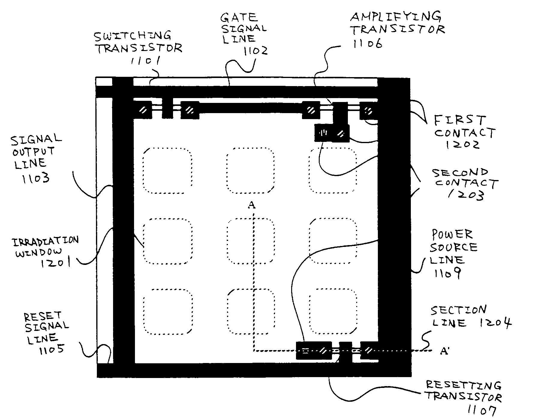
[0121]Next, a description will be given of an example when a plurality of irradiation windows are provided to a single pixel. FIG. 11 shows a circuit diagram of a pixel. In FIG. 11, there is used a photodiode 1104 as a photoelectric conversion element which is an active type sensor. A P-channel side terminal of the photodiode 1104 is connected to a power source reference line 1112 and an N-channel side terminal 1113 thereof is connected to a gate terminal of an amplifying transistor 1106. A drain terminal and a source terminal of the amplifying transistor 1106 are connected to a power source line 1109 and a drain terminal of a switching transistor 1101. Agate terminal of the switching transistor 1101 is connected with a gate signal line 1102 and a source terminal thereof is connected with a signal output line 1103. A gate terminal of a resetting transistor 1107 is connected to a reset signal line 1105. A source terminal and a drain terminal of the resetting transistor 1107 are conne...


PUM


Abstract

To provide a close contact type sensor promoting a light utilizing efficiency, there is provided a close contact type sensor featured in that in a close contact type sensor having a sensor circuit portion and an irradiation window portion, a plurality of the irradiation windows are arranged and positions and sizes of the irradiation windows are matched to positions and sizes of opening portions of LCD utilized as a light source.

Description

CROSS-REFERENCE TO RELATED APPLICATIONS[0001]This application is a divisional application of U.S. application Ser. No. 09 / 849,975, filed May 8, 2001 now abandoned, which claims the benefit of a foreign priority application filed in Japan as Serial No. 2000-135239 on May 8, 2000. This application claims priority to each of these prior applications, and the disclosures of the prior applications are considered part of (and are incorporated by reference in) the disclosure of this application.BACKGROUND OF THE INVENTION[0002]1. Field of the Invention[0003]The present invention relates to a close contact type sensor. More in details, the present invention relates to an MOS type sensor apparatus formed by using TFT above a glass substrate.[0004]2. Description of the Related Art[0005]In recent years, information apparatus such as personal computers have spread widely and there has been an increase in request of reading various information by a personal computer as electronic information. Th...

Claims


Application Information

Patent Timeline
Patent Type & Authority Patents(United States)
IPC IPC(8): G01J1/42H04N1/04G06T1/00H01L21/77H01L21/84H01L27/12H01L27/146H04N1/028H04N1/19
CPCH01L27/14645H01L27/14609H01L27/12H01L27/1214
Inventor KIMURA, HAJIME
Owner SEMICON ENERGY LAB CO LTD
Why Eureka
Try Eureka