Wavelength conversion device and related light-emitting device thereof
a conversion device and wavelength technology, applied in the field of display and illumination technologies, can solve the problems of reducing the reflectivity and thermal stability the effectiveness of the reflective layer is significantly reduced, and the conventional led and halogen light source is increasingly unsatisfactory for the high power and high brightness requirements of display and illumination applications, so as to reduce the penetration depth of light, and reduce the thickness of the reflective layer.
- Summary
- Abstract
- Description
- Claims
- Application Information
AI Technical Summary
Benefits of technology
Problems solved by technology
Method used
Image
Examples
first embodiment
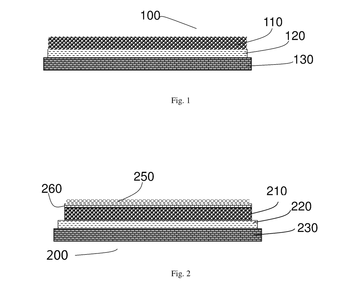
[0033]Refer to FIG. 1, which illustrates the structure of a wavelength conversion device according to a first embodiment of the present invention. As shown in the figure, the wavelength conversion device 100 includes a substrate 130, a light emitting layer 110, and a reflective layer 120. The reflective layer 120 includes reflective particles, auxiliary particles, and a first binder. The light emitting layer 110 includes a wavelength conversion material and a second binder.
[0034]As discussed in the background section, the light emitted by the light emitting layers is incident on the reflective layer, and reflected by it back to the light emitting layer. The heat generated by the light emitting layer is transmitted by the reflective layer to the substrate, and then dissipated.
[0035]In the wavelength conversion device 100, the reflective layer 120 has two functions, namely, light reflection and heat conduction. The reflective layer 120 should has a relatively high reflectivity, to ens...
second embodiment
[0056]Refer to FIG. 2, which illustrates the structure of a wavelength conversion device according to a second embodiment of the present invention. In the wavelength conversion device 200 of this embodiment, the light emitting layer 210, the reflective layer 220 and the substrate 230 are the same as those of the first embodiment and will not be described in further detail. A difference from the first embodiment is that, as shown in FIG. 2, the wavelength conversion device 200 further includes a glass layer 260 and an antireflection film 250.
[0057]The glass layer 260 is located on the light emitting layer 210, and is formed from a third glass powder. Because the surface of the light emitting layer 210 may have a small amount of wavelength conversion material particles that protrude from the surface, coating directly on such a surface may cause the coated film to be non-smooth. But if the light emitting layer is polished before coating, the light emitting layer may be damaged by the p...
third embodiment
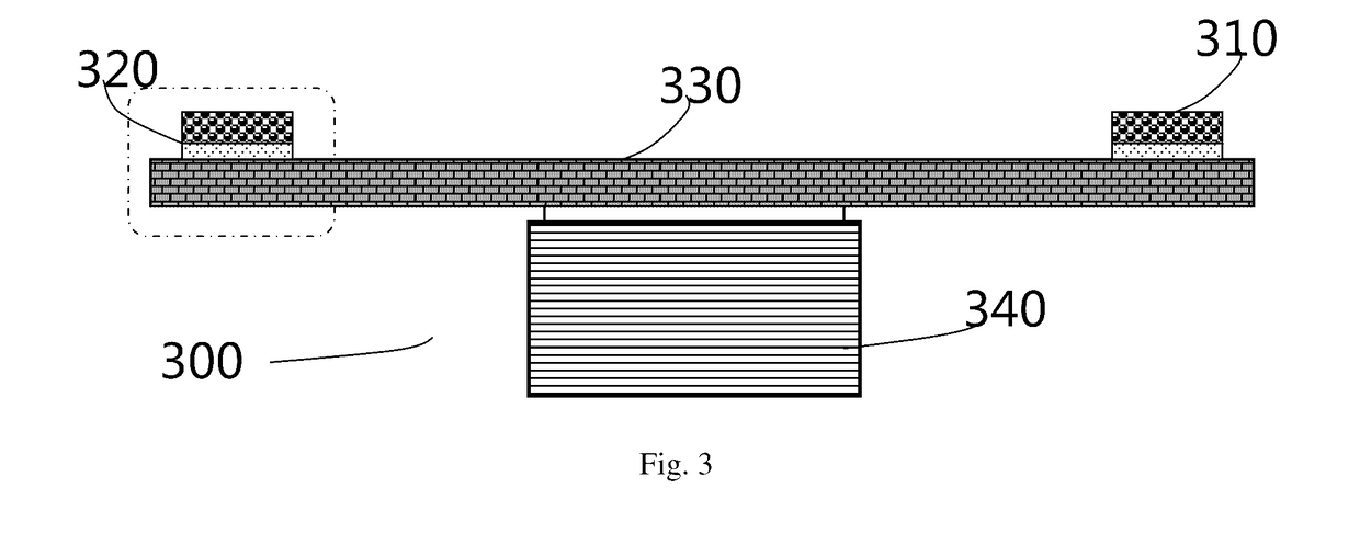
[0060]Refer to FIG. 3, which illustrates the structure of a wavelength conversion device according to a third embodiment of the present invention. In the wavelength conversion device 300 of this embodiment, the light emitting layer 310, the reflective layer 320 and the substrate 330 are the same as those of the first embodiment and will not be described in further detail. A difference from the first embodiment is that this embodiment further includes a drive device 340. Specifically, the drive device 340 is a drive motor. The substrate 330 in this embodiment is a round substrate, which carries the ring shaped reflective layer 320 and light emitting layer 310. The drive device 340 is fixedly coupled to the substrate 330. When the drive device 340 rotates, it drives the substrate 330 and the reflective layer 320 and the light emitting layer 310 on the substrate to rotate. This avoids the problem when the laser from the excitation light source continuously illuminates on the same point...
PUM
| Property | Measurement | Unit |
|---|---|---|
| mass fraction | aaaaa | aaaaa |
| mass fraction | aaaaa | aaaaa |
| particle diameter | aaaaa | aaaaa |
Abstract
Description
Claims
Application Information


