Non-volatile memory device with threshold voltage control function

a non-volatile memory and threshold voltage technology, applied in static storage, digital storage, instruments, etc., can solve the problems of inability to accurately read out data accumulated in memory cell transistors, inability to uniformly perform rewrite operations for all erase unit areas, and inability to improve the number of rewrite operations.

Inactive Publication Date: 2007-10-09
PANASONIC CORP
View PDF7 Cites 79 Cited by
  • Summary
  • Abstract
  • Description
  • Claims
  • Application Information

AI Technical Summary

Benefits of technology

[0020]Therefore, an object of the present invention is to provide a non-volatile memory device in which the number of rewrite operations is improved for all erase unit areas even when the number of rewrite operations varies among erase unit areas.
[0021]To achieve the object, the present invention provides an electrically erasable and programmable non-volatile memory device comprising a plurality of erase unit areas each including a plurality of non-volatile memory cell transistors which are simultaneously selected in an erase operation, a plurality of output regulating value storing sections provided corresponding to the respective erase unit areas, of storing output regulating values of the respective erase unit areas in a non-volatile manner, a voltage generating circuit of generating a voltage having a level required in an erase operation and a write operation with respect to each of the erase unit areas, a voltage regulating circuit of regulating the level of the voltage generated in the voltage generating circuit based on a corresponding one of the output regulating values provided thereto, a read determination circuit of performing determination with respect to data after an erase operation and a write operation with respect to each of the erase unit areas, and a control circuit of operating in an erase operation and a write operation with respect to each of the erase unit areas. Therefore, for an erase unit area having a large number of rewrite operations, the apparent characteristics of the memory cell transistor are maintained to be in a satisfactory state by updating the output regulating value, while for an erase unit area having a small number of rewrite operations, updating of the output regulating value can be suppressed. Therefore, even when the number of rewrite operations varies among erase unit areas, it is possible to prevent unnecessary electrical stress from being given to an erase unit area having a small number of rewrite operations, and improve the number of rewrite operations for all erase unit areas.
[0022]In this case, the read determination circuit may perform the determination step in accordance with a criterion stricter than when a read operation is performed. When performing the determination step, the read determination circuit may apply to a current detection type sense amplifier circuit a reference current which provides a criterion stricter than when a read operation is performed. Alternatively, the read determination circuit may apply to the memory cell transistor a gate voltage which provides a criterion stricter than when a read operation is performed. Thereby, a degradation in the characteristics of a memory cell transistor can be detected at an earlier stage, so that an erase operation and a write operation can be more reliably performed with respect to the memory cell transistor.

Problems solved by technology

When these threshold voltages depart from correct values in their respective initial states, data accumulated in the memory cell transistor can be no longer correctly read out.
However, a rewrite operation with respect to a memory cell transistor may not be uniformly performed for all erase unit areas, i.e., the number of rewrite operations may vary among erase unit areas.
Therefore, when the number of rewrite operations varies among erase unit areas, the number of rewrite operations may not be satisfactorily improved.
However, when an excessive erase / write voltage is applied to a memory cell transistor, the overall amount of electricity passing through a tunnel oxide film provided below the floating gate of the memory cell transistor increases, so that an electric field higher than necessary is applied.

Method used


Image

  • Non-volatile memory device with threshold voltage control function
  • Non-volatile memory device with threshold voltage control function
  • Non-volatile memory device with threshold voltage control function

Examples


first embodiment

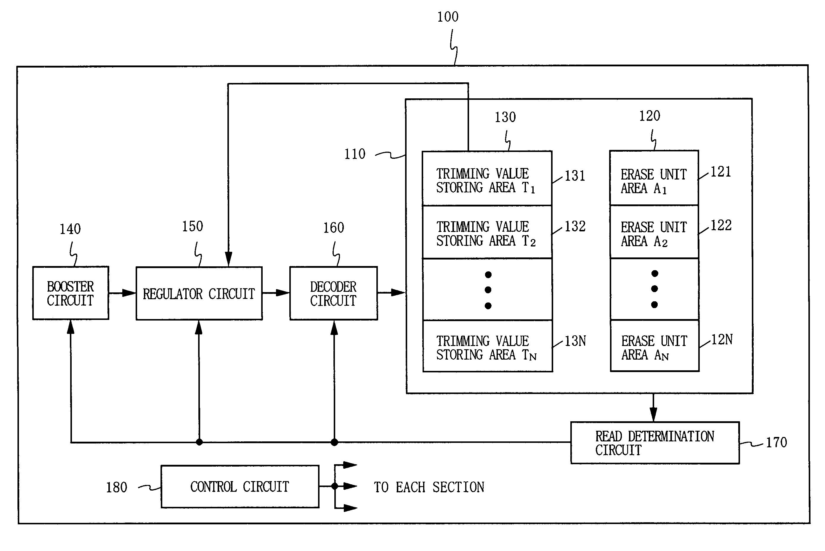
[0054]FIG. 1 is a diagram illustrating a structure of a flash EEPROM according to a first embodiment of the present invention. The flash EEPROM 100 of FIG. 1 comprises a memory cell array 110, a booster circuit 140, a regulator circuit 150, a decoder circuit 160, a read determination circuit 170, and a control circuit 180. The memory cell array 110 includes N erase unit areas 121 to 12N, and N trimming value storing areas 131 to 13N. Among these components, the booster circuit 140 functions as a voltage generating circuit, the regulator circuit 150 functions as a voltage regulating circuit, and the trimming value storing areas 131 to 13N function as output regulating value storing sections.

[0055]The memory cell array 110 includes a plurality of memory cell transistors arranged in an array. Each memory cell transistor has a floating gate for accumulating electric charge so as to store data in a non-volatile manner. The memory cell transistor is subjected to a step of injecting electr...

second embodiment

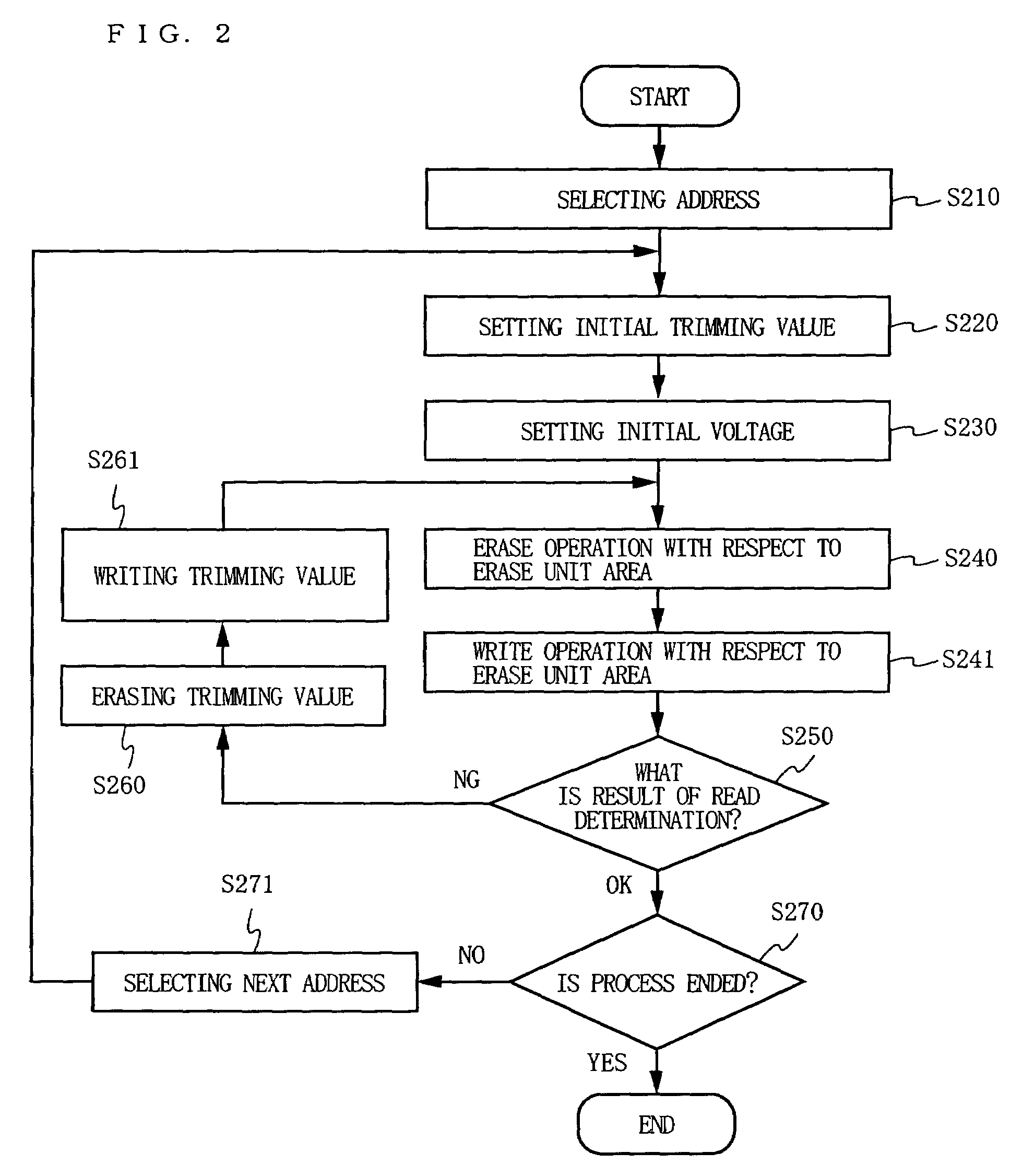
[0078]A flash EEPROM according to a second embodiment of the present invention has the same structure as that of the first embodiment (see FIG. 1). FIG. 3 is a flowchart illustrating a rewrite operation in the flash EEPROM of the second embodiment. This flowchart is obtained by replacing step S260 with step S360 in the flowchart of FIG. 2.

[0079]The flash EEPROM of the second embodiment is different from the flash EEPROM of the first embodiment in the following. In the flash EEPROM of the second embodiment, the regulator circuit 150 outputs a higher level of post-regulation erase / write voltage as the number of “0”s included in an input trimming value is increased.

[0080]In the flash EEPROM of the first embodiment, a trimming value is erased in step S260. By contrast, in the flash EEPROM of the second embodiment, a trimming value is erased only in the first performance of step S360 (i.e., only when step S360 is performed for the first time with respect to a selected trimming value) as ...

third embodiment

[0086]FIG. 4 is a diagram illustrating a structure of a flash EEPROM according to a third embodiment of the present invention. The flash EEPROM 400 of FIG. 4 is obtained by adding a trimming value temporarily holding circuit 405 to the flash EEPROM of the second embodiment. FIG. 5 is a flowchart illustrating a rewrite operation in the flash EEPROM 400 of the third embodiment. This flowchart is obtained by shifting steps S260 and S361 of the flowchart of FIG. 3 to steps S560 and S561, and adding step S551 to the original positions of steps S260 and S361.

[0087]The flash EEPROM of the third embodiment is different from the flash EEPROM of the second embodiment in the following. The flash EEPROM 400 of the third embodiment comprises the trimming value temporarily holding circuit 405 in addition to the components of the flash EEPROM of the second embodiment. The trimming value temporarily holding circuit 405 is a volatile memory section composed of, for example, a CMOS circuit or the lik...


PUM


Abstract

Even when the number of rewrite operations varies among erase unit areas, the number of rewrite operations is improved for all of the erase unit areas. A flash EEPROM 100 comprises a trimming value storing area 130 of storing a trimming value corresponding to each erase unit area 120 included in a memory cell array 110. When an erase operation and a write operation are performed with respect to a certain erase unit area 120, a regulator circuit 150 converts a voltage boosted by a booster circuit 140 to a level corresponding to the trimming value for the erase unit area 120. When a read determination circuit 170 detects an abnormality as the number of rewrite operations is increased, the trimming value is updated to a value which causes the regulator circuit 150 to increase the output voltage.

Description

BACKGROUND OF THE INVENTION[0001]1. Field of the Invention[0002]The present invention relates to an electrically erasable and programmable non-volatile memory device. More particularly, the present invention relates to a non-volatile memory device in which a threshold voltage is controlled to relax electrical stress with respect to a memory cell transistor, thereby improving the number of rewrite operations.[0003]2. Description of the Background Art[0004]As electrically erasable and programmable non-volatile memory devices, EEPROM (Electrically Erasable Programmable Read Only Memory) and flash EEPROM are known, as disclosed in, for example, Japanese Patent Laid-Open Publication No. 2002-208291. FIG. 19 is a diagram illustrating a structure of a flash EEPROM described in the above-described publication. The flash EEPROM 1900 of FIG. 19 comprises a memory cell array 1910, a booster circuit 140, a regulator circuit 150, a decoder circuit 160, a read determination circuit 170, and a con...

Claims


Application Information

Patent Timeline
Patent Type & Authority Patents(United States)
IPC IPC(8): G11C11/34
CPCG11C16/30G11C16/102
Inventor MISUMI, KENJIKOJIMA, MAKOTO
Owner PANASONIC CORP
Why Eureka
Try Eureka