Flexible scheme for configuring programmable semiconductor devices using or loading programs from SPI-based serial flash memories that support multiple SPI flash vendors and device families

a technology of serial flash memory and spi flash, which is applied in the direction of pulse technique, instruments, computation using denominational number representation, etc., can solve the problems of interface not easily supporting random access into the memory array, high cost of comparable densities, and low data transfer performance, so as to simplify board testing and manufacturing, reduce fpga configuration costs, and improve data transfer performance

Active Publication Date: 2007-10-09
XILINX INC
View PDF9 Cites 70 Cited by
  • Summary
  • Abstract
  • Description
  • Claims
  • Application Information

AI Technical Summary

Benefits of technology

[0023]The SPI-based configuration logic of the present invention is similar to that which exists for Xilinx serial PROMs. This SPI-based configuration logic can therefore readily co-exist with the present Xilinx serial configuration scheme. The high-density SPI flash devices can potentially reduce FPGA configuration costs by up to 80%.
[0025]In accordance with another embodiment, an interface between a JTAG unit on the PLD can be configured to allow the SPI flash to be programmed and verified through the PLD's JTAG pins, thereby simplifying board testing and manufacturing. Even without a special interface between the JTAG and SPI interfaces, it is possible to toggle the SPI pins via the JTAG interface, albeit slowly. The purpose of any special interface logic would be to improve data transfer performance.
[0026]Note that connections from within the PLD advantageously allow the SPI interface to be re-used to connect to the wide variety of SPI-based peripheral components.

Problems solved by technology

However, although SPI-based serial flash devices share the same four-wire interface, each vendor and each vendor device family uses a slightly different command protocol that prevents users from easily using multiple vendors.
The primary disadvantage of SSA PROM devices, when compared to SPI flash memories, is that they are generally more expensive for comparable densities.
Consequently, they are manufactured in higher production volumes by multiple vendors, resulting in a price-competitive market environment.
Because of its serial sequential nature, the interface does not easily support random access into to the memory array.
The primary disadvantages of I2C-based PROMs are that they typically have lower densities and significantly lower communications bandwidth (400 kHz vs.

Method used


Image

  • Flexible scheme for configuring programmable semiconductor devices using or loading programs from SPI-based serial flash memories that support multiple SPI flash vendors and device families
  • Flexible scheme for configuring programmable semiconductor devices using or loading programs from SPI-based serial flash memories that support multiple SPI flash vendors and device families
  • Flexible scheme for configuring programmable semiconductor devices using or loading programs from SPI-based serial flash memories that support multiple SPI flash vendors and device families

Examples


Embodiment Construction

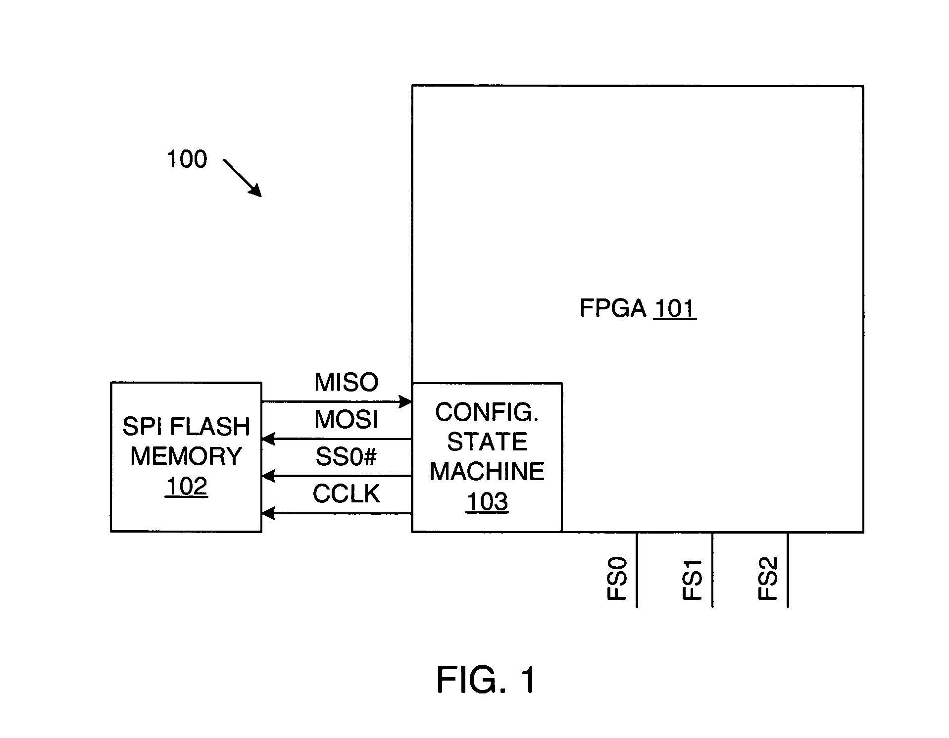
[0032]FIG. 1 is a block diagram of a system 100 that includes programmable logic device (PLD) 101 and an associated SPI-based flash memory device 102. In the described embodiments, PLD 101 is an SRAM-based field programmable gate array (FPGA). However, the present invention is applicable to other types of programmable devices, including but not limited to microcontrollers or embedded processors. FPGA 101 includes a configuration state machine 103 and input / output pins FS0, FS1 and FS2.

[0033]In general, system 100 operates as follows.

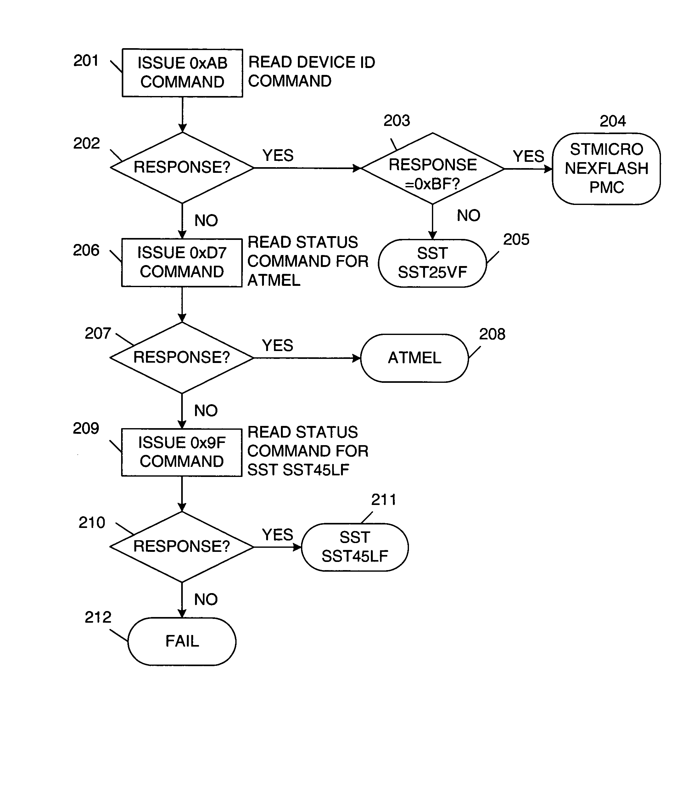
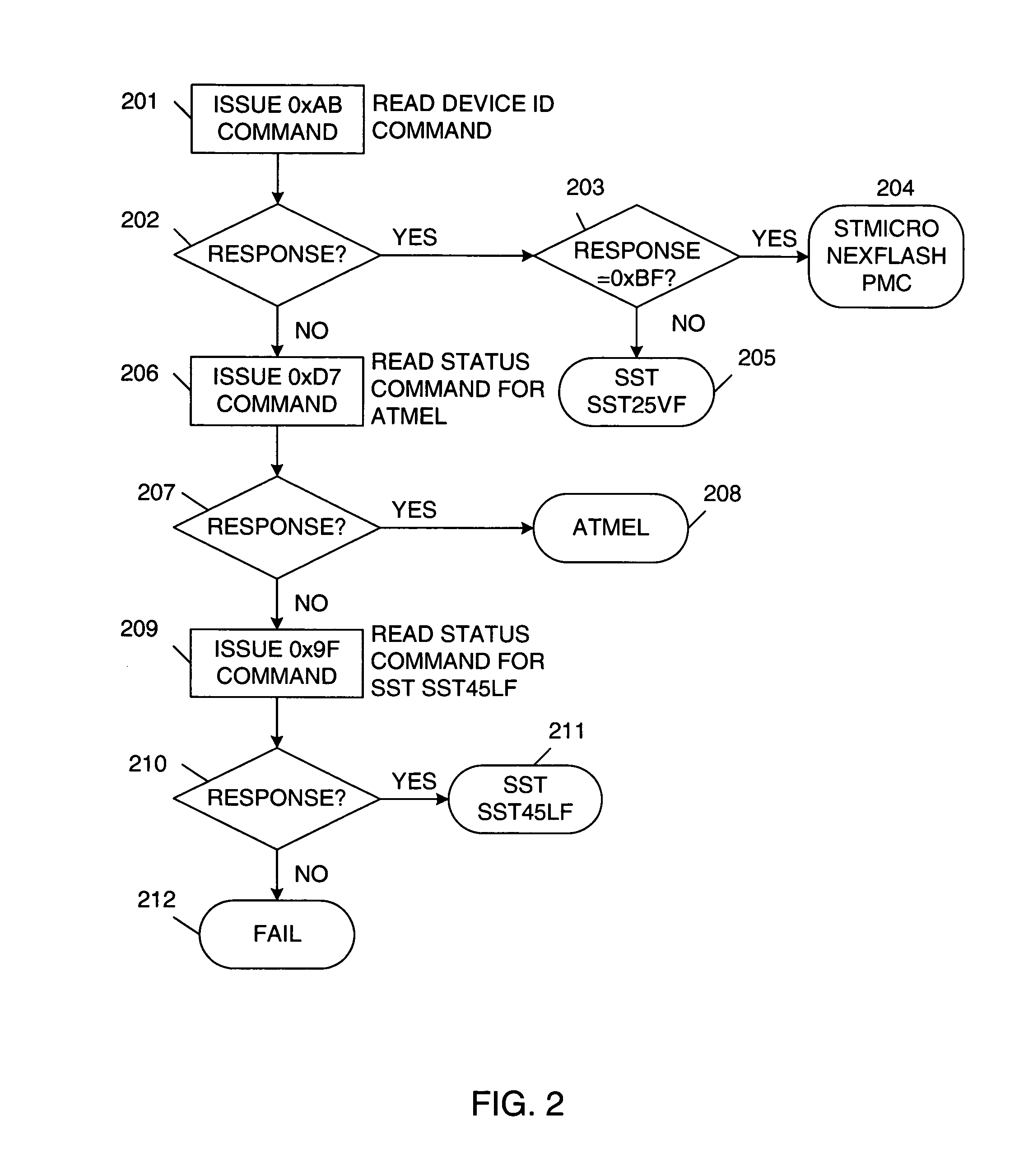
[0034]First, FPGA 101 identifies the vendor and device family of the attached SPI-based memory device 102.

[0035]Second, FPGA 101 issues the correct read command, typically unique for the identified SPI-based memory device 102, including the starting address, and any dummy bytes, if required by the SPI flash device used in the application.

[0036]Third, FPGA 101 continuously reads the configuration data from the SPI memory device 102, either until the FPGA ...


PUM


Abstract

A method and structure for configuring a programmable logic device (PLD) from a serial peripheral interface (SPI) based serial memory. The type of the SPI memory is initially identified by the PLD. The PLD then selects the appropriate read command in response to the SPI memory type. The PLD then issues the read command to the SPI memory. In response, the SPI memory continuously provides a set of configuration data to the PLD. The PLD is configured in response to the configuration data. The PLD can identify the SPI memory type in response to control signals on pins of the PLD. Alternately, the PLD can identify the SPI memory type by performing a search. The search can include issuing a plurality of known read commands to the SPI memory, and then determining which read command causes the SPI memory to respond.

Description

FIELD OF THE INVENTION[0001]The present invention uses the commercially available, low-cost, high density serial flash memories offered by multiple vendors that use the four wire serial peripheral interface (SPI) communication protocol to provide a cost effective configuration storage device for configuring programmable semiconductor devices, or for loading configuration or application programs for stand-alone or embedded processors, digital signal processors, or microcontrollers.RELATED ART[0002]Programmable logic devices, such as field programmable gate arrays (FPGAs), typically include an array of configuration memory cells that are loaded with configuration data values. These configuration data values control the configuration of the programmable logic device. The configuration data values are initially stored in an external memory device, such as a programmable read only memory (PROM). The configuration data values are transferred from the external memory device to the programm...

Claims


Application Information

Patent Timeline
Patent Type & Authority Patents(United States)
IPC IPC(8): G06F12/00
CPCH03K19/17772H03K19/17748H03K19/1776H03K19/17744G11C16/20G11C2216/30
Inventor KNAPP, STEVEN K.
Owner XILINX INC
Why Eureka
Try Eureka