Printed circuit board including embedded chips and method of fabricating the same using plating

a technology of printed circuit boards and embedded chips, which is applied in the direction of printed circuit non-printed electric components association, sustainable manufacturing/processing, and final product manufacturing, etc., can solve the problems of large product size, large high frequency noise generation, and reducing the performance and reliability of the system

Inactive Publication Date: 2007-10-16
SAMSUNG ELECTRO MECHANICS CO LTD
View PDF8 Cites 108 Cited by
  • Summary
  • Abstract
  • Description
  • Claims
  • Application Information

AI Technical Summary

Benefits of technology

[0048]Accordingly, the present invention has been made keeping in mind the above problems occurring in the related art, and an object of the present invention is to provide a method of fabricating a PCB including embedded chips, in which a plating process is used to fix a chip to a central layer when the central layer is formed, so that the subsequent processes are easily performed.
[0049]Another object of the present invention is to provide a method of fabricating a PCB including embedded chips, in which electrical inspection of the connection state of the chips of the central layer is performed to easily correct errors before other layers are laminated on the central layer.
[0050]A further object of the present invention is to provide a PCB including embedded chips and a method of fabricating the same, in which solder need not be used to electrically connect the chips, and hence, noise due to the solder is not generated.
[0051]Still another object of the present invention is to provide a PCB including embedded chips and a method of fabricating the same, in which electrical connection properties of the chips embedded in the PCB are improved.

Problems solved by technology

However, as the speed of the component increases, voltage fluctuation of a power line occurs, resulting in the generation of a lot of high frequency noise, such as SSN (Simultaneous Switching Noise) or delta-I (ΔI).
The high frequency noise (e.g., SSN) causes system delay or a logic fault, thereby decreasing the performance and reliability of the system.
In such cases, the first and second conventional techniques are disadvantageous because the space between the electrical component and the insulating layer as the central layer is large, and thus, the resultant product has a large size.
Further, the first and second conventional techniques are disadvantageous because the space between the chip and the copper foil layer is large, and thus, efficient radiating effects cannot be obtained.
Furthermore, the second conventional technique is disadvantageous because a build-up process used for lamination takes a long time.
However, the third conventional technique is disadvantageous in that because the through holes filled with conductive ink adhere to the chip upon simultaneous lamination, the alignment of the layers cannot be accurately controlled.
Moreover, since the radiation takes place using the radiating pattern, limitations are imposed on fabricating a high density circuit due to the formation of a passage required for emission of the radiating pattern.
However, since the chip condenser is simply embedded in the core layer by means of a conductive adhesive, the above method has problems similar to conventional methods of fabricating PCBs including embedded chips.

Method used


Image

  • Printed circuit board including embedded chips and method of fabricating the same using plating
  • Printed circuit board including embedded chips and method of fabricating the same using plating
  • Printed circuit board including embedded chips and method of fabricating the same using plating

Examples


Embodiment Construction

[0061]Hereinafter, a detailed description will be given of the present invention, with reference to the appended drawings.

[0062]FIGS. 4A to 4G sequentially show a process of forming a central layer in the fabrication method of a PCB including embedded chips, according to the present invention.

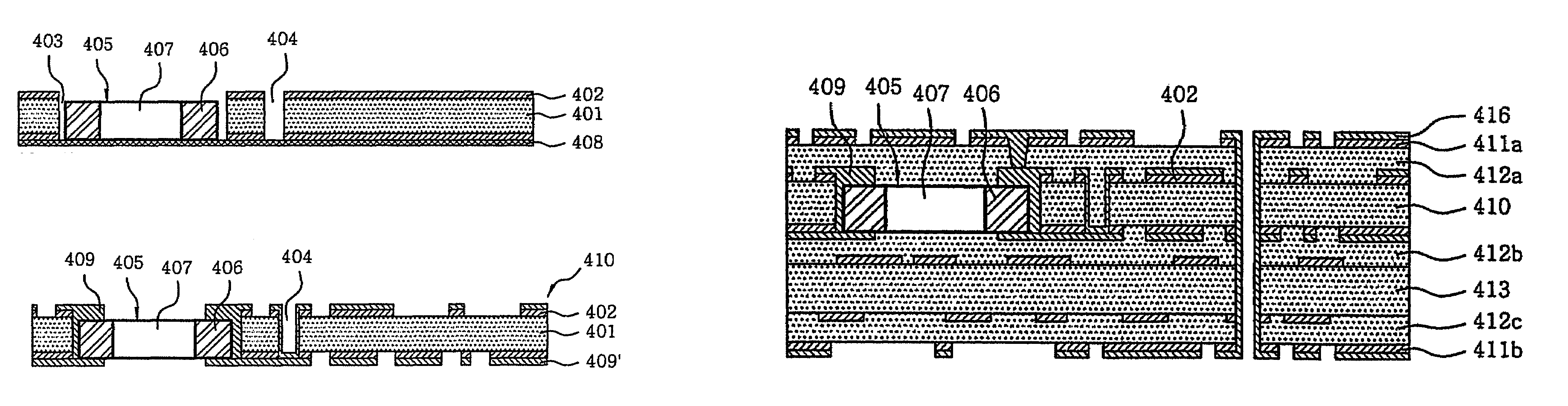
[0063]In FIG. 4A, a copper clad laminate (CCL) 400 is prepared, which has an insulating resin layer 401 and copper foil layers 402 formed on both surfaces thereof. In this case, the CCL 400 is preferably exemplified by a glass / epoxy CCL having an insulating layer that is formed of an epoxy resin (a mixture of a resin and a curing agent) impregnated into glass fiber and a copper foil layer formed thereon.

[0064]In FIG. 4B, a hollow portion 403, into which a chip is to be inserted, and a via hole 404 are formed through the CCL 400. The formation of the hollow portion 403 and the via hole 404 is preferably carried out by a mechanical drilling process, such as a CNC drilling process. Also, a laser d...


PUM


Abstract

A method of fabricating a printed circuit board (PCB) including embedded chips, composed of forming a hollow portion for chip insertion through a substrate, inserting the chip into the hollow portion, fixing the chip to the substrate by use of a plating process to form a central layer having an embedded chip, and then laminating a non-cured resin layer and a circuit layer having a circuit pattern on the central layer. Also, a PCB including embedded chips fabricated using the above method is provided.

Description

INCORPORATION BY REFERENCE[0001]The present application claims priority under 35 U.S.C. §119 to Korean Patent Application No.: 10-2004-0116809 filed on Dec. 30, 2004. The content of the application is incorporated herein by reference in its entirety.BACKGROUND OF THE INVENTION[0002]1. Field of the Invention[0003]The present invention relates, generally, to a printed circuit board (PCB) including embedded chips, and a fabricating method thereof. More particularly, the present invention relates to a method of fabricating a PCB including embedded chips, including forming a hollow portion for chip insertion through a substrate, inserting the chip into the hollow portion, fixing the chip to the substrate by use of a plating process to form a central layer having an embedded chip, and then laminating a non-cured resin layer and a circuit layer having a circuit pattern on the central layer; and a PCB including embedded chips fabricated by the above method.[0004]2. Description of the Relate...

Claims


Application Information

Patent Timeline
Patent Type & Authority Patents(United States)
IPC IPC(8): H01L21/44H01L21/48
CPCH01L24/18H01L24/82H05K1/185H01L23/5389H01L21/4857H01L2924/014H01L2224/18H01L2924/01005H01L2924/01015H01L2924/01027H01L2924/01029H01L2924/01033H01L2924/01078H01L2924/01082H01L2924/14H01L2924/19041H01L2924/19042H01L2924/19043H01L2924/30105H01L2924/30107H01L2924/3025H05K3/4623H05K3/4652H05K2201/09509H05K2201/10636H05K2201/10674H01L2924/01006H01L24/19H01L2224/04105H01L2224/73267H01L2224/92244Y02P70/50H05K1/18H05K3/30
Inventor CHO, SUK HYEONRYU, CHANG SUPLEE, DOO HWAN
Owner SAMSUNG ELECTRO MECHANICS CO LTD
Why Eureka
Try Eureka