Method for detecting and correcting defective pixels in a digital image sensor

a digital image sensor and defective technology, applied in the field of image processing, can solve the problems of erasing local ridges in the image, inaccurate sensor values, and many defective pixels in the digital image sensor, so as to reduce false bad pixel detection, avoid erasing fine vertical lines, and reduce false bad detection.

Active Publication Date: 2007-10-16
APTINA IMAGING CORP
View PDF9 Cites 51 Cited by
  • Summary
  • Abstract
  • Description
  • Claims
  • Application Information

AI Technical Summary

Benefits of technology

[0010]Embodiments of the present invention provide a bad pixel correction (BPC) algorithm for detecting and correcting defective pixels in a digital color image sensor. For a current pixel, gradients from neighboring pixels in at least one other color plane than the color plane of the current pixel are used to determine whether the current pixel is defective. For example, both the gradients and a range of sensor values from neighboring pixels in the same color plane as the current pixel can be determined. If the sensor value of the current pixel is outside of the range by a threshold amount that is calculated using one or more of the gradients, the current pixel is determined to be a defective pixel. The gradients in other color planes provide a more accurate prediction of the sensor value of the current pixel by considering the local roughness in the image (e.g. a textured region vs. a uniform region).
[0013]Advantageously, using gradients in more than one color plane reduces false bad pixel detection by accounting for local ridges in the image. In addition, false bad detection can be further reduced by using both vertical and diagonal gradients to avoid erasing fine vertical lines. As a further advantage, in some embodiments, the BPC algorithm requires only additions, subtractions, shifts and comparison, all of which are easy to implement in hardware. Therefore, the BPC algorithm can be implemented on the same chip as the sensor, while also being effective in accurately detecting and correcting the defective pixels. Furthermore, the invention provides embodiments with other features and advantages in addition to or in lieu of those discussed above. Many of these features and advantages are apparent from the description below with reference to the following drawings.

Problems solved by technology

Despite advances in the manufacturing process, digital image sensors often contain a few defective pixels as a result of noise or fabrication errors, such as impurity contamination.
Defective pixels respond inappropriately to the incident light, and therefore produce inaccurate sensor values.
However, the Maynants & Diercickx BPC method does not compare pixels in other color planes that are spatially adjacent to the current pixel, and therefore has the drawback of erasing local ridges in the image, where sensor values peak or recess.
The Maynants & Diercickx BPC method also does not compare pixels vertically, and therefore has the additional drawback of erasing fine vertical lines.
However, the Tan & Acharya method requires the storage of the bad pixel map in non-volatile memory.
Incorporating non-volatile memory into an image sensor or an image processor chip is a significant expense.
Furthermore, the Tan & Acharya method also does not compare pixels in other color planes when creating the bad pixel map.

Method used


Image

  • Method for detecting and correcting defective pixels in a digital image sensor
  • Method for detecting and correcting defective pixels in a digital image sensor
  • Method for detecting and correcting defective pixels in a digital image sensor

Examples


Embodiment Construction

[0025]The numerous innovative teachings of the present application will be described with particular reference to exemplary embodiments. However, it should be understood that these embodiments provide only a few examples of the many advantageous uses of the innovative teachings herein. In general, statements made in the specification do not necessarily delimit any of the various claimed inventions. Moreover, some statements may apply to some inventive features, but not to others.

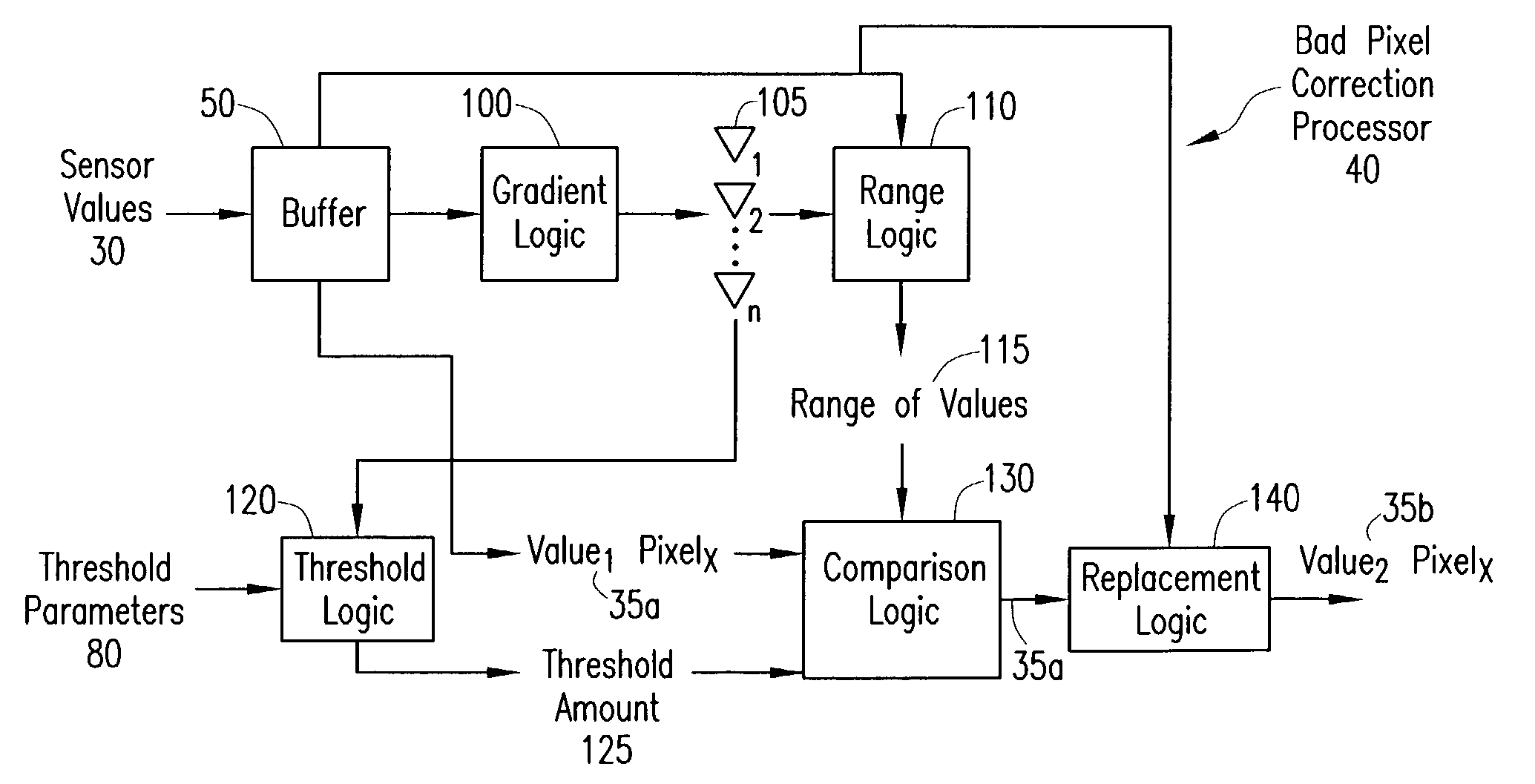
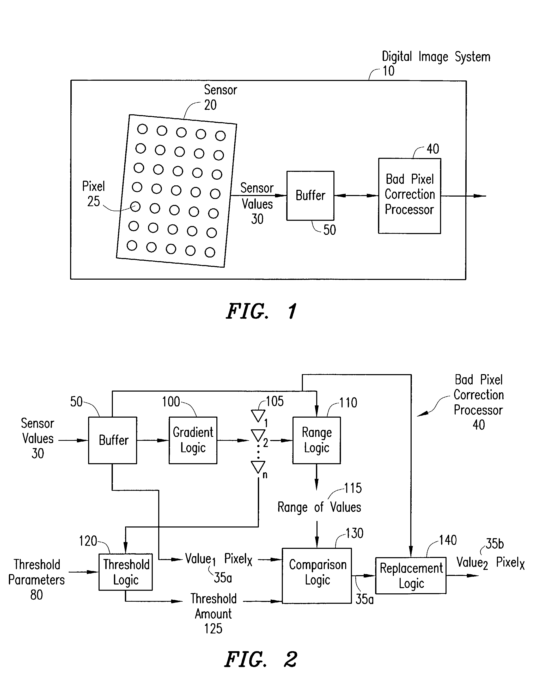
[0026]FIG. 1 shows a digital image system 10 implementing a bad pixel correction (BPC) algorithm 40 in accordance with the present invention. The digital image system 10 can be any digital imaging device, such as a digital camera, video camera, medical imaging device, etc. The digital image system 10 can also be a computer system, such as a personal computer or server, having a memory therein for storing image data. Thus, the BPC algorithm 40 can be within a digital imaging device or a part of an image proce...


PUM


Abstract

A bad pixel correction (BPC) algorithm that can be implemented on the image sensor chip is provided for detecting and correcting defective pixels in a digital color image sensor. Gradients of neighboring pixels in at least one other color plane than the color plane of a current pixel and a range of sensor values from neighboring pixels in the same color plane as the current pixel are determined. If the sensor value of the current pixel is outside of the range by a threshold amount that is calculated using one or more of the gradients, the current pixel is determined to be a defective pixel, and replaced using the sensor values of the neighboring pixels in the same color plane.

Description

BACKGROUND OF THE INVENTION[0001]1. Technical Field of the Invention[0002]The present invention relates generally to digital color image sensors, and specifically to image processing of sensor values.[0003]2. Description of Related Art[0004]Electronic image sensors are predominately of two types: CCDs (Charge Coupled Devices) and CMOS—APS (Complimentary Metal Oxide Semiconductor—Active Pixel Sensors). Both types of sensors typically contain an array of photo-detectors (e.g., pixels), arranged in a pattern, that sample color within an image. Each pixel measures the intensity of light within one or more ranges of wavelengths, corresponding to one or more perceived colors.[0005]Despite advances in the manufacturing process, digital image sensors often contain a few defective pixels as a result of noise or fabrication errors, such as impurity contamination. Defective pixels respond inappropriately to the incident light, and therefore produce inaccurate sensor values. Defective pixels ar...

Claims


Application Information

Patent Timeline
Patent Type & Authority Patents(United States)
IPC IPC(8): H04N9/64H04N3/14G06T1/00G06T3/40H04N1/40H04N5/367H04N5/369H04N9/07
CPCH04N5/367H04N2209/045H04N25/68
Inventor KAKARALA, RAMAKRISHNAZHANG, XUEMEIYING, BOND YU-PONGSTANBACK, JOHN H.
Owner APTINA IMAGING CORP
Why Eureka
Try Eureka