Chip resistor and method of manufacturing the same

a technology of resistor and chip, which is applied in the direction of resistor details, resistive material coating, instruments, etc., can solve the problems of resistance likely to change, and achieve the effect of increasing the length of the insulating substrate, increasing the size and weight of products, and reducing the possibility of producing defective products

Active Publication Date: 2007-10-23
ROHM CO LTD
View PDF13 Cites 9 Cited by
  • Summary
  • Abstract
  • Description
  • Claims
  • Application Information

AI Technical Summary

Benefits of technology

[0011]With the structure disclosed in the Patent Document 1 (FIG. 13), the winding shape of the resistor film 5′ provided by the two inward grooves 7′, 8′ and the two trimming grooves 9′, 10′ increases the length of the current path, whereby the surge resistance is reliably improved while keeping the size and weight of the chip resistor small.

Problems solved by technology

Generally, a chip resistor having a resistor film formed on an insulating substrate in the form of a chip has a drawback that its resistance is likely to change when surge voltage generated due to the influence of static electricity or power supply noise is applied.

Method used


Image

  • Chip resistor and method of manufacturing the same
  • Chip resistor and method of manufacturing the same
  • Chip resistor and method of manufacturing the same

Examples


first embodiment

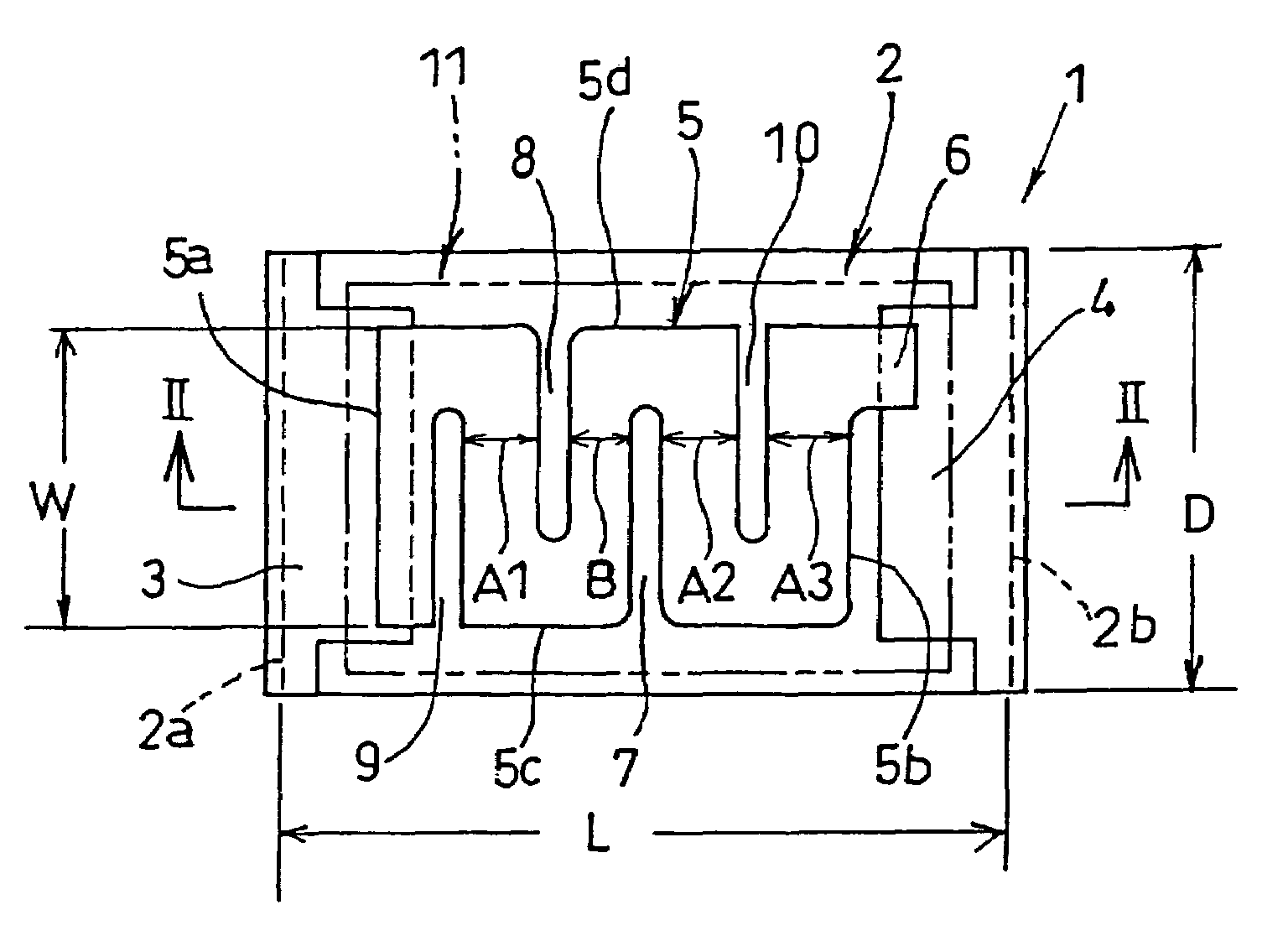
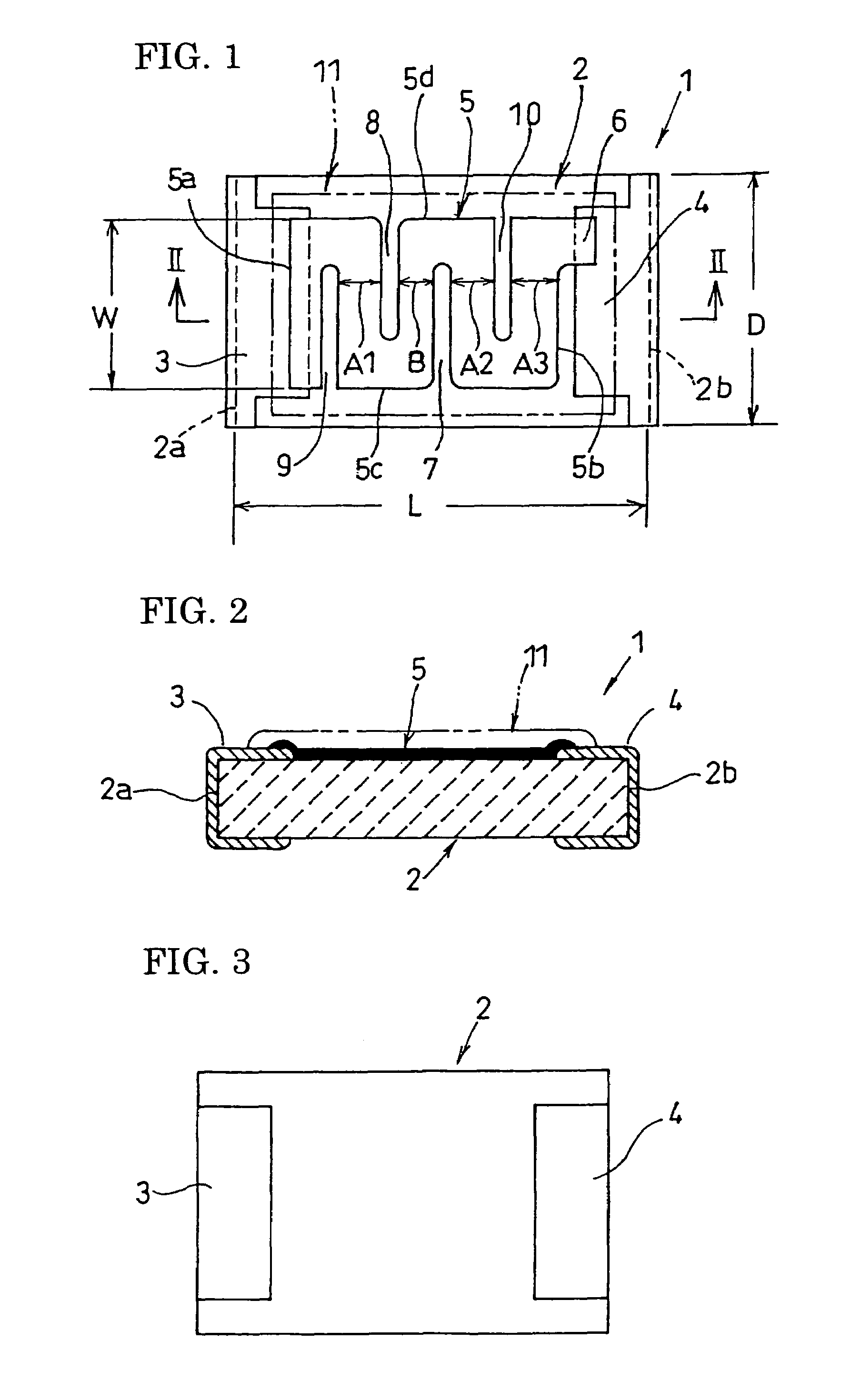
[0050]FIGS. 1 and 2 show a chip resistor 1 according to the present invention.

[0051]The chip resistor 1 includes an insulating substrate 2 in the form of an elongated rectangular chip having a width D and a length L, terminal electrodes 3 and 4 formed on the upper surface of the insulating substrate at longitudinally opposite ends thereof, and a resistor film 5 having a width W and formed on the upper surface of the insulating substrate 2 to extend longitudinally of the insulating substrate 2 between the terminal electrodes 3 and 4. The resistor film is formed by screen printing and the subsequent baking of the material.

[0052]The resistor film 5 has a first and a second end edges 5a and 5bSpecifically, in screen printing the resistor film, the first end edge 5a of the resistor film 5 is formed to overlap and to be connected to the terminal electrode 3 throughout the width W, whereas a narrow portion 6 is provided integrally at the second end edge 5b of the resistor film 5. Of a firs...

second embodiment

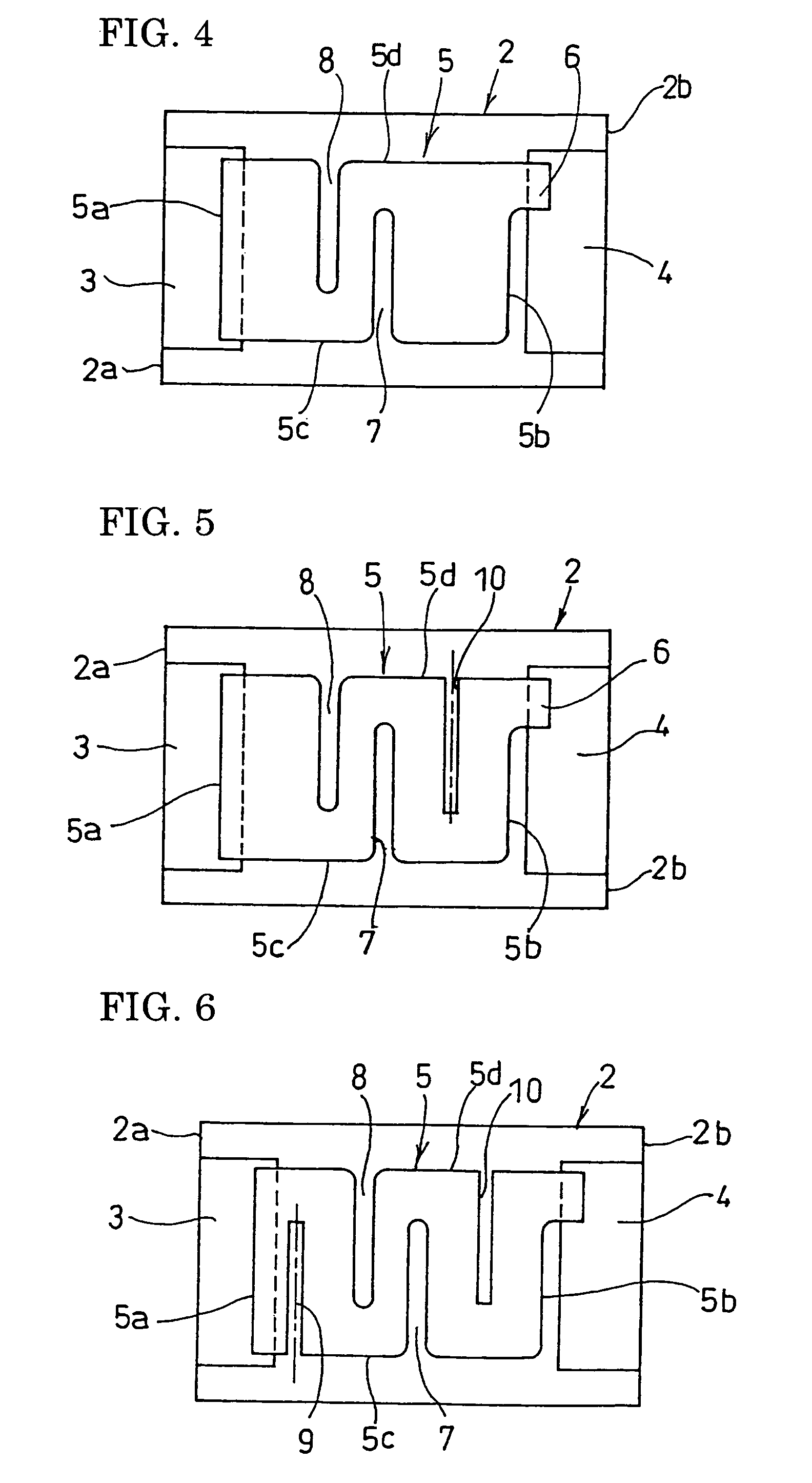
[0066]FIGS. 7 and 8 show a chip resistor 21 according to the present invention.

[0067]The chip resistor 21 includes an insulating substrate 22 in the form of an elongated rectangular chip having a width D and a length L, terminal electrodes 23 and 24 formed on the upper surface of the insulating substrate at longitudinally opposite ends thereof, and a resistor film 25 having a width W and formed on the upper surface of the insulating substrate 22 to extend longitudinally of the insulating substrate 22 between the terminal electrodes 23 and 24. The resistor film is formed by screen printing and the subsequent baking of the material.

[0068]The resistor film 25 has a first and a second end edges 25a and 25b. Specifically, in screen printing the resistor film, a first narrow portion 26 is provided integrally at the first end edge 25a of the resistor film 25. Of a first and a second longitudinal edges 25c and 25d of the resistor film 25, the first narrow portion 26 is provided at the first...


PUM


Abstract

A chip resistor is provided which includes a resistor film 5 formed between a pair of terminal electrodes 2 and 3 on an upper surface of an insulating substrate 2. The resistor film is formed with two inward grooves 7, 8 and two trimming grooves 9, 10 which are alternately provided for causing the current path in the resistor film to have a winding shape. The two inward grooves 7 and 8 are provided approximately at the midpoint between one end edge 5a and the other end edge 5b of the resistor film 5. The trimming groove 9 is provided between the inward groove 8 and the end edge 5a of the resistor film, whereas the other trimming groove 10 is provided between the inward groove 7 and the end edge 5b of the resistor film, whereby the time required for the trimming adjustment to adjust the resistance to a predetermined value is shortened, and the yield rate is reduced to reduce the cost.

Description

TECHNICAL FIELD[0001]The present invention relates to a chip resistor comprising a resistor film formed on an insulating substrate in the form of a chip. The invention particularly relates to a chip resistor having improved surge resistance and to a method of manufacturing such a chip resistor.BACKGROUND ART[0002]Generally, a chip resistor having a resistor film formed on an insulating substrate in the form of a chip has a drawback that its resistance is likely to change when surge voltage generated due to the influence of static electricity or power supply noise is applied. It is known that the change of resistance due to surge voltage can be suppressed by increasing the length of the current path in the resistor film.[0003]The Patent Documents 1 and 2 as the prior art disclose chip resistors designed to improve the surge resistance.[0004]Specifically, as shown in FIG. 13, the chip resistor 1′ disclosed in the Patent Document 1 includes an insulating substrate 2′ in the form of a c...

Claims


Application Information

Patent Timeline
Patent Type & Authority Patents(United States)
IPC IPC(8): H01C1/012H01C3/12H01C7/00H01C17/26
CPCH01C3/12H01C17/267H01C7/003H01C7/00H01C17/06H01C17/22H01C17/24
Inventor YONEDA, MASAKI
Owner ROHM CO LTD
Why Eureka
Try Eureka