
Ba-based blue phosphor material provided with a particle surface coating and plasma display panel using the same

Inactive Publication Date: 2007-10-30
PANASONIC CORP
View PDF15 Cites 5 Cited by
  • Summary
  • Abstract
  • Description
  • Claims
  • Application Information

AI Technical Summary

Benefits of technology

[0009]In other words, a phosphor of the present invention includes a blue phosphor having a crystal structure of Ba1−xMgAl10O17:Eux or Ba1−x−ySryMgAl10O17:Eux and exited by ultraviolet light to emit visible light. In the blue phosphor, the vicinity of the side faces of layers containing Ba atoms is coated with an oxide or a fluorine-containing oxide. This structure can inhibit water adsorption onto the surface of the blue phosphor, decrease luminance degradation and chromaticity shift of the phosphor, or improve discharge characteristics thereof.
[0010]Further, a method of manufacturing a phosphor of the present invention includes: a mixed solution fabrication step in which a metal salt or an organometalic salt containing elements constituting a blue phosphor is mixed with an aqueous medium, to fabricate a mixed solution; a step of drying the mixed solution and thereafter firing the mixture, to fabricate a phosphor of Ba1−xMgAl10O17:Eux or Ba1−x−ySryMgAl10O17:Eux; surface-treating this phosphor in an acescent aqueous solution; and coating the vicinity of the side faces of layers containing Ba atoms in this phosphor with SiO2, Al2O3, ZnO, MgAl2O4, La2O3, LaPO4, Zn2SiO4, Si(O—F)2, La2(O—F)3, or Al2(O—F)3. Adding a step of coating the side faces of Ba—O layers to the process of fabricating a blue phosphor can provide a phosphor durable against water and carbonic acid gas, without causing degradation of the luminance of the blue phosphor.
[0011]Further, a plasma display device of the present invention has a plasma display panel in which a plurality of discharge cells of one or a plurality of colors are disposed in arrays, phosphor layers having a color corresponding to the respective discharge cells are disposed, and the phosphor layers are excited by ultraviolet light to emit light. The phosphor layers include blue phosphor layers. The blue phosphor constituting each blue phosphor layer is made of a compound represented by Ba1−xMgAl10O17:Eux or Ba1−x−ySryMgAl10O17:Eux in which the vicinity of the side faces of layers containing Ba atoms is coated with at least one material of SiO2, Al2O3, ZnO, MgAl2O4, La2O3, LaPO4, Zn2SiO4, Si(O—F)2, La2(O—F)3, and Al2(O—F)3. This structure can provide a plasma display device having improved luminance, inhibited luminance degradation and chromaticity shift, and excellent luminance characteristics.

Problems solved by technology

However, the smaller diameters of phosphor particles increase the specific surface area of the phosphor and thus defects on the surface of the phosphor.
This poses problems of luminance degradation and chromaticity shift (color shift and image bum caused by the chromaticity shift), or decrease in drive voltage margin and increase in discharge voltage.
However, coating the entire surface of a phosphor poses another problem: the thin layer of coating absorbs ultraviolet light and thus decreases the emission luminance of the phosphor.

Method used


Image

  • Ba-based blue phosphor material provided with a particle surface coating and plasma display panel using the same
  • Ba-based blue phosphor material provided with a particle surface coating and plasma display panel using the same
  • Ba-based blue phosphor material provided with a particle surface coating and plasma display panel using the same

Examples


examples

[0087]In order to evaluate the performance of a plasma display device of the present invention, samples based on the preferred embodiment were produced and performance evaluation tests were performed on the samples. The experimental results are described below.

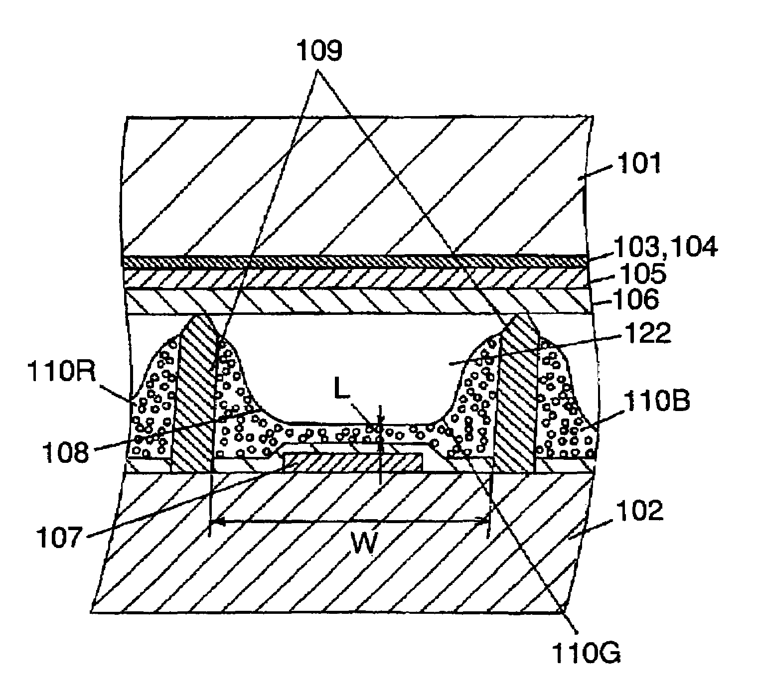
[0088]Each of the plasma display devices produced has a diagonal size of 42 in. (for a HDTV screen having a rib pitch of 150 μm). Each of the plasma display devices was produced so that the dielectric glass layer was 20 μm thick, the MgO protective layer was 0.5 μm thick, and the distance between the display electrode and the display scan electrode was 0.08 mm. The discharge gas filling discharge space essentially consists of neon and. contains 5% of xenon gas mixed therein.

[0089]Used as the blue phosphor particles of each of Sample Nos. 1 though 10 for the plasma display devices is a phosphor in which the vicinity of the side faces of Ba—O layers is coated with an oxide or a fluorine-containing oxide. The synthesis conditions...

experiment 1

[0096]Model experiments were performed on Sample Nos. 1 through 10 and Comparative Sample Nos. 11, 12, and 13 to determine luminances and luminance degradation factors. In the model experiments, these phosphors were fired (520° C., 20 min.) in the rear panel manufacturing process to determine how the luminance of each color changed. The luminance of the particles before firing and the luminance of the applied paste after firing were measured. The luminance degradation factor of each color obtained before and after firing was measured.

experiment 2

[0097]Measured was the luminance degradation factor of each phosphor obtained before and after the panel sealing step (at 450° C. for 20 min.) in the panel manufacturing process.


PUM


Abstract

A phosphor in which water adsorption onto the surface of a blue phosphor is inhibited, luminance degradation and chromaticity shift of the phosphor is decreased, or discharge characteristics thereof is improved, and a plasma display device using the phosphor. In phosphor layers used for plasma display, selectively coating at least the vicinity of the sides of planes of mirror symmetry containing Ba atoms in a blue phosphor with an oxide or a fluorine-containing oxide inhibits water adsorption onto the surface of the blue phosphor, decreases luminance degradation and chromacity shift of a phosphor, or improves discharge characteristics thereof.

Description

TECHNICAL FIELD[0001]The present invention relates to a plasma display device used for image display on a television, or other equipment, and particularly to a phosphor constituting phosphor layers for use in the plasma display device.BACKGROUND ART[0002]Among color display devices used for image display on a computer screen or television, a display device using a plasma display panel (hereinafter referred to as a “PDP”) has recently been drawing attention, as a large, thin, and lightweight color display device.[0003]A plasma display device using a PDP performs additive color mixing of so-called three primary colors (red, green, and blue) to provide full-color display. For the full-color display, a plasma display device has phosphor layers for emitting the respective three primary colors, i.e. red (R), green (G), and blue (B). Phosphor particles constituting these phosphor layers are exited by ultraviolet light generated in discharge cells of the PDP to generate visible light of res...

Claims


Application Information

Patent Timeline
IPC IPC(8): H01J17/49H01J1/62H01J63/04C09K11/64C09K11/02C09K11/08C09K11/77H01J9/22H01J11/22H01J11/24H01J11/34H01J11/42
CPCC09K11/025C09K11/7734H01J2211/42C09K11/64C09K11/08H01J11/42H01J9/22
Inventor KAWAMURA, HIROYUKIAOKI, MASAKISUGIMOTO, KAZUHIKOOTANI, MITSUHIROHIBINO, JUNICHI
Owner PANASONIC CORP
Learn More