Method and apparatus for supporting a semiconductor wafer during processing

a technology of semiconductor wafers and supporting devices, applied in electrical devices, chemical vapor deposition coatings, coatings, etc., can solve the problems of difficult control, difficult to heat a semiconductor wafer, and a relatively long time to heat a wafer, etc., to achieve the effect of short tim

Inactive Publication Date: 2007-12-25
ASM INTERNATIONAL
View PDF50 Cites 271 Cited by
  • Summary
  • Abstract
  • Description
  • Claims
  • Application Information

AI Technical Summary

Benefits of technology

[0009]The aim of the present invention is to provide a method with which contactless heating of semiconductor substrates to relatively high temperature within a relatively short time is possible.
[0011]Surprisingly, it has been found that if the spacing between the side sections, or between side section and wafer, is set to be relatively small, particularly rapid heat transfer can take place. It is possible to achieve heating to far about 1000° C. within a few seconds. Because with this arrangement the wafer, in principle, does not have to be supported, but is held accurately and definitively in its place by the gas streams, the wafer will also not be subjected to stresses generated by local temperature differences and distortion will be prevented as far as possible. Incidentally, it is pointed out that if a slight degree of distortion does take place, the stabilizing effect of the gas streams in opposing directions is such that the wafer is pressed straight in a ‘gentle’ manner without damage.
[0012]Therefore, it is now possible to keep the apparatus at the process temperature and load the wafer while the side sections are at process temperature without damage for the wafer. As a consequence, a particularly small peak power is needed to achieve such rapid heating of wafer because the energy required to heat the wafer is withdrawn from the side sections. It will be understood that the method described above is outstandingly suitable for processes in which wafers are treated one-by-one (‘single wafer processing’). However, it is also possible to treat large numbers of wafers one after the other or parallel to one another in the manner described above.
[0016]With the method according to the invention it is possible to prevent these problems. This is because, according to a further embodiment of this method, a temperature difference is applied over the wafer. One of the side sections is heated to a relatively high temperature, whilst the other of the side sections is heated to a relatively low temperature. It has been found that, as a result of the thermal behavior of the enclosing apparatus, the wafer will assume a temperature which is dependent on the position of the wafer with respect to the two heated side sections. If the two side sections are equidistant from the wafer and the same gas is present on both sides, the temperature will fairly accurately be the average of the values of the temperatures of each of the side sections.
[0020]It has been found that the rate of deposition of, for example, polysilicon from silane on a substrate is lower by a factor of 350 at 700 K and a partial pressure of 0.4 torr than at 900 K. This means that by controlling the temperature, deposition is negligible on the side section from which the process gas is supplied and which is at low temperature.
[0023]With the method according to the invention, these values can be set very accurately. After all, it has been found that these values are mainly dependent on the position of the wafer in the enclosing apparatus. As already indicated above, the position of the wafer in the tunnel-like apparatus is accurately related to the quantity and type of gas supplied from the related side sections.

Problems solved by technology

Secondly, it takes a relatively long time to heat a wafer.
Such a method is particularly expensive and difficult to control.
This apparatus has the drawback that due to the presence of many metal parts with complicated constructions in close proximity to the wafer, only heating to limited temperatures is possible.
Due to the succession of columns, where the wafer is supported, and gaps between the columns where the wafer is exposed to the heat radiation of the lamps, both the support of the wafer and the heating are not homogeneous.
It has been found that only limited heating can take place effectively by heating the gases, as is described in the above-mentioned Netherlands applications.

Method used


Image

  • Method and apparatus for supporting a semiconductor wafer during processing
  • Method and apparatus for supporting a semiconductor wafer during processing
  • Method and apparatus for supporting a semiconductor wafer during processing

Examples


Embodiment Construction

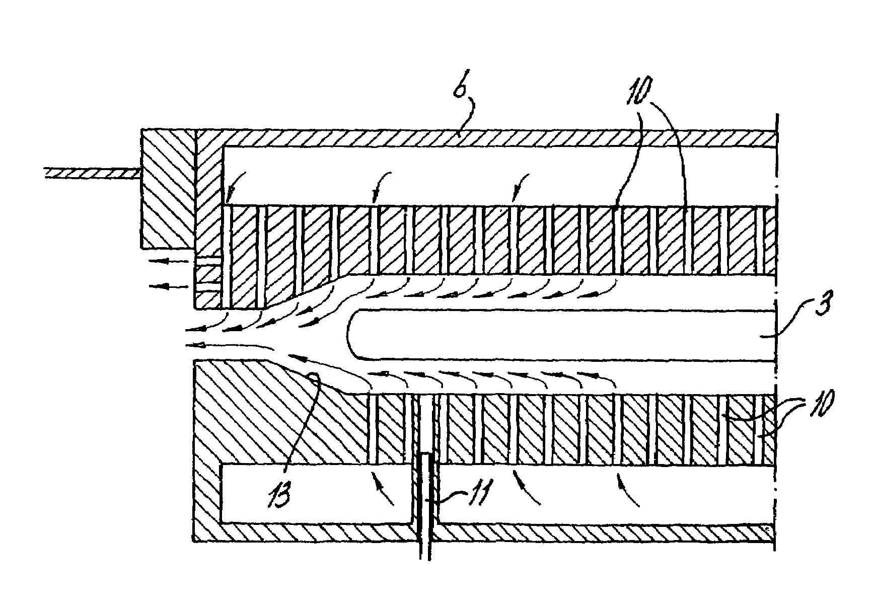
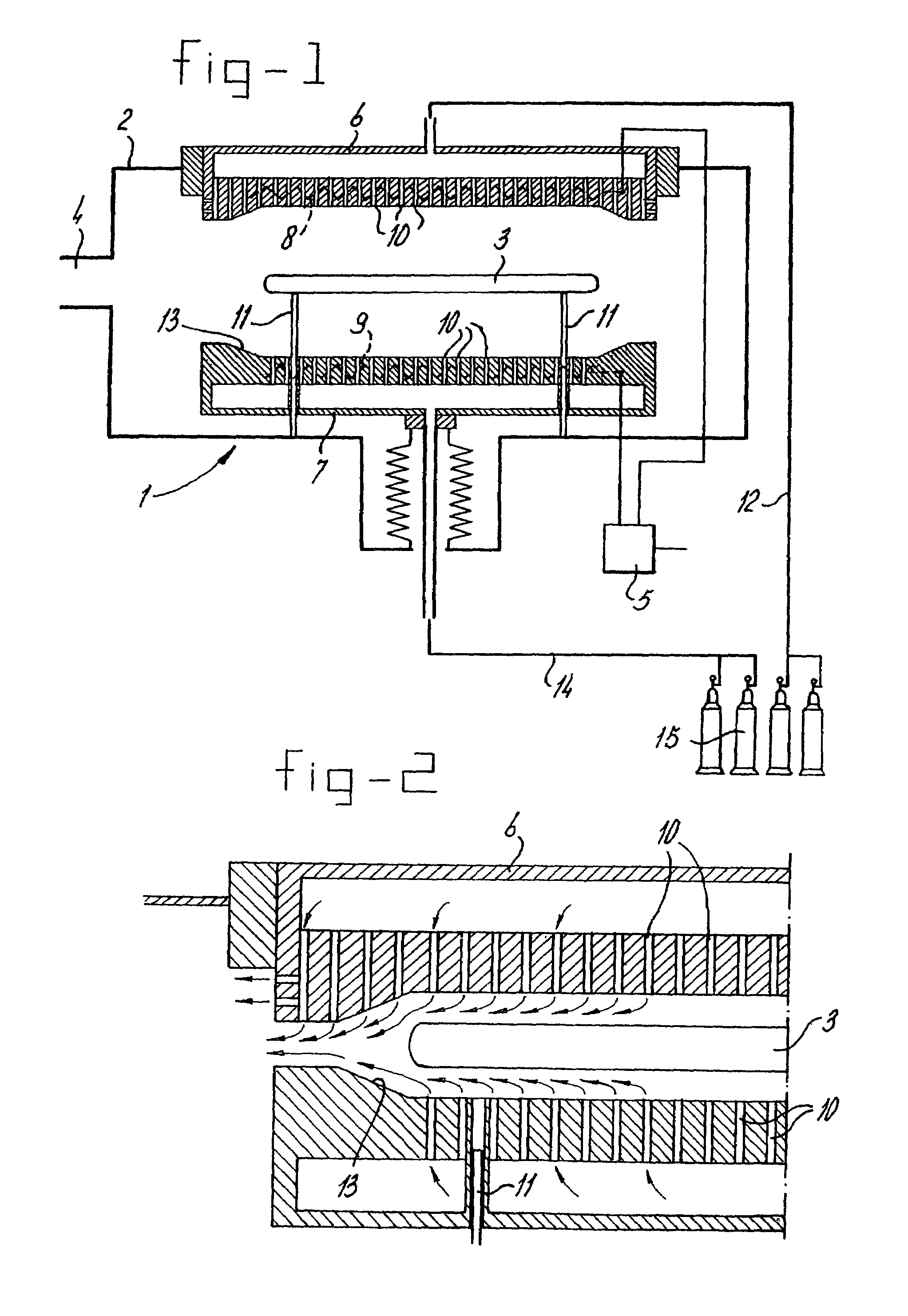
[0031]In FIG. 1, the apparatus according to the invention is indicated in its entirety by 1. This apparatus is provided with an inlet 4, which can be connected, in a manner not shown in more detail, to a ‘load lock’ or a cluster system for further treatment of semiconductor substrates.

[0032]The actual apparatus according to the invention, consisting of top and bottom or first and second side sections 6 and 7, respectively, is accommodated in a pressure vessel 2 for carrying out a process in a specific environment or under elevated or reduced pressure.

[0033]The first side section 6 is joined rigidly to the pressure vessel 2. A heating coil 8, which is connected to a control 5, is mounted inside the first side section. A gas supply line 12 is also present, which gas supply line is connected to the gas feeds 10 which comprise a number of uniformly distributed passages.

[0034]It must be understood that in practice a very much larger number of passages will generally be used, which passag...


PUM

PropertyMeasurementUnit
temperatureaaaaaaaaaa
temperaturesaaaaaaaaaa
thicknessaaaaaaaaaa

Abstract

A semiconductor wafer is processed while being supported without mechanical contact. Instead, the wafer is supported by gas streams emanating from a large number of passages in side sections positioned very close to the upper and lower surface of the wafer. The gas heated by the side sections and the heated side sections themselves quickly heat the wafer to a desired temperature. Process gas directed to the “device side” of the wafer can be kept at a temperature that will not cause deposition on that side section, but yet the desired wafer temperature can be obtained by heating non-process gas from the other side section to the desired temperature. A plurality of passages around the periphery of the wafer on the non-processed side can be employed to provide purge gas flow that prevents process gas from reaching the non-processed side of the wafer and the adjacent area of that side section.

Description

RELATED APPLICATIONS[0001]This application is a continuation of U.S. application Ser. No. 10 / 603,515, filed Jun. 24, 2003, now U.S. Pat. No. 6,805,749 which is a continuation of U.S. application Ser. No. 09 / 717,702, filed Nov. 20, 2000 (now U.S. Pat. No. 6,613,685 B1, issued Oct. 2, 2003), which is a continuation of U.S. application Ser. No. 09 / 227,564, filed Jan. 8, 1999 (now U.S. Pat. No. 6,183,565, issued Feb. 6, 2001), which is a continuation-in-part of International application No. PCT / NL97 / 00398, filed Jul. 8, 1997, which claims priority from Netherlands Patent Appln. No. 1003538, filed Jul. 8, 1996.BACKGROUND OF THE INVENTION[0002]The present invention relates to a method for contactless treatment of a substrate such as a semiconductor wafer, comprising enclosing the wafer in an apparatus and applying two gas streams, in opposing directions, from first and second side sections located opposite on another, to the two opposing planar sides or surfaces of the wafers.[0003]A meth...

Claims


Application Information

Patent Timeline
Patent Type & Authority Patents(United States)
IPC IPC(8): H01L21/302C23C16/44C23C16/455C23C16/458H01L21/00H01L21/677H01L21/683
CPCC23C16/45521C23C16/458C23C16/4583H01L21/6838H01L21/67109H01L21/67784C23C16/46C23C16/45597C23C16/45565
Inventor GRANNEMAN, ERNST HENDRIK AUGUSTHUUSSEN, FRANK
Owner ASM INTERNATIONAL
Why Eureka
Try Eureka