Method for local wafer thinning and reinforcement

a local wafer and reinforcement technology, applied in semiconductor/solid-state device testing/measurement, semiconductor/solid-state device details, instruments, etc., can solve the problems of reducing the physical integrity of the entire wafer, reducing the thickness of the doped layer, and difficult to image the dut through a thick doped silicon layer, etc., to achieve the effect of maintaining the integrity of the wafer

Inactive Publication Date: 2008-01-01
DCG SYST
View PDF19 Cites 3 Cited by
  • Summary
  • Abstract
  • Description
  • Claims
  • Application Information

AI Technical Summary

Benefits of technology

[0007]Various embodiments of the present invention provide a method for locally thinning a semiconductor wafer, while maintaining the integrity of the wafer.
[0010]According to an illustrative method of the invention for preparing a semiconductor wafer for testing, the method proceeds using the steps of: selecting a die to be tested; measuring the length of a large diagonal of said die; thinning a circular area over said die, the circular area having a diameter larger than said large diagonal; mounting an insert in said circular area; and, applying an adhesive in a peripheral area of the insert so as not to obscure the optical path to the die. In one specific aspecxt of the invention the circular area comprises a slanted wall. According to another aspect the circular area comprises a vertical wall, and the diameter of the insert is smaller than the diameter of the circular area. According to yet another aspect, the circular area comprises a wall having a wall chamfer provided therein, and the insert comprises a mating chamfer having a thickness larger than thickness of the wall chamfer. In any of the embodiments of the invention, the insert may beneficially and advantageously be made of undoped silicon.
[0011]According to another aspect of the invention, a semiconductor wafer that is pre-prepared for optical testing is provided, the wafer comprising: a wafer substrate having a thickness T and a plurality of dies fabricated thereupon, each die having a boundary delineated by scribe lines; at least one thinned area over one of said dies, said thinned area having a boundary extending beyond the scribe lines of said die, said circular area reducing the thickness of said wafer substrate to a thickness t small than thickness T; an insert provided inside said thinned area; and, an adhesive provided on the periphery of said insert so as not to obscure the optical path to the die. In one aspect the area comprises a slanted wall. In another aspect the area comprises a circular area having a vertical wall, and wherein the diameter of said insert is smaller than the diameter of the circular area. According to yet another aspect, the area comprises a wall having a wall chamfer provided therein, and wherein said insert comprises a mating chamfer having a thickness larger than thickness of the wall chamfer. In any of the aspect described, the insert may beneficially and advantageously comprise silicon.
[0013]An advantage of the inventive method is that it help maintain the physical integrity of the thinned wafer. Another advantage of the inventive method is that it maintains the index of refraction the same throughout the optical path.

Problems solved by technology

Since doped silicon generally absorbs photon illumination, it is very difficult to image the DUT through a thick doped silicon layer.
On the other hand, thinning the entire wafer to 100 micron would drastically reduce its physical integrity and will probably cause breakage.
Consequently, using such an insert causes optical aberration.
Moreover, the adhesive used to glue the insert may introduce additional aberrations—depending on its index of refraction.
While the adhesive may be selected so its index of refraction matches that of the glass insert, the combination would still introduce aberrations since the glass insert and adhesive will not match to the doped silicon of the DUT.

Method used


Image

  • Method for local wafer thinning and reinforcement
  • Method for local wafer thinning and reinforcement
  • Method for local wafer thinning and reinforcement

Examples


Embodiment Construction

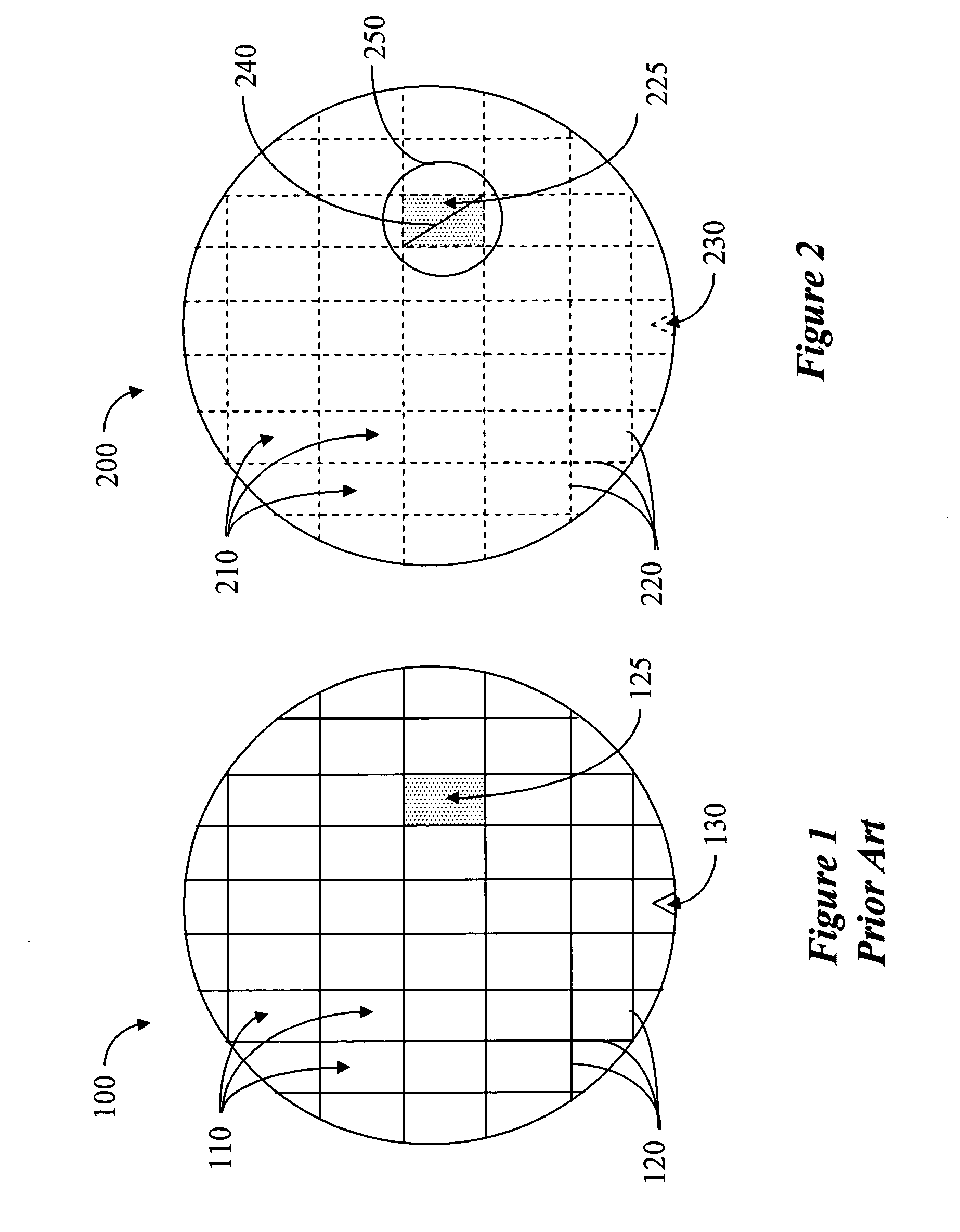
[0025]An embodiment of the invention will now be described in details with reference to FIGS. 2 and 3. In FIG. 2, wafer 200 is shown from the backside thereof, as indicated by scribe lines 220 being drawn in broken line format. The die 225, that is selected to be inspected, is again shown shaded. As is known, dies 225 would normally be a square or a rectangle having a long diagonal 240. Upon selection of the die to be inspected, its long diagonal 240 is measured. Then, a circular area to be thinned is determined, having a diameter which is larger than the measured diagonal.

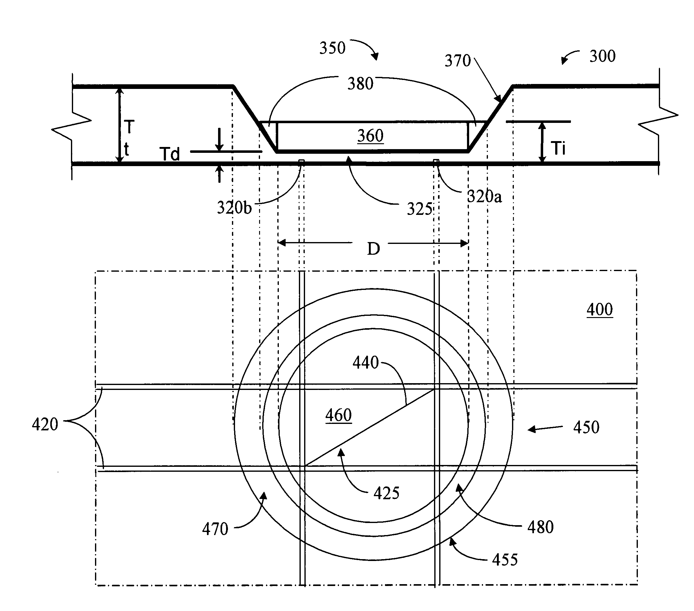
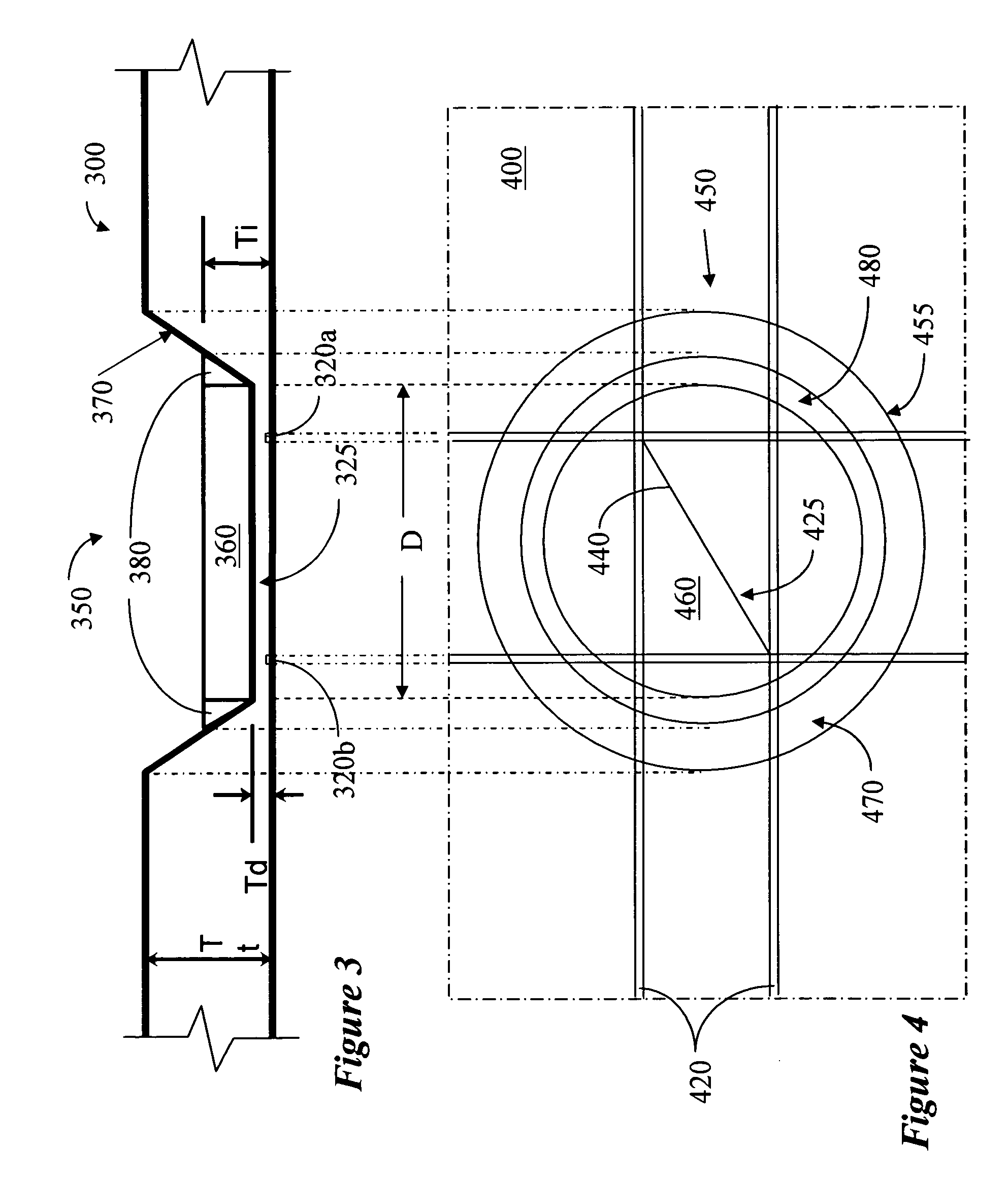
[0026]FIG. 3 is a partial cross-section of a wafer 300 prepared according to one embodiment of the invention. In FIG. 3, the boundaries of die 325 are marked by scribe lines 320a and 320b. The total thickness, Tt, of the wafer is on the order of several hundreds of microns, e.g., 650 microns. An area 350 over die 325 is thinned to a thickness Td of about 100 microns. As is shown, the area 350 has a diameter, D, wh...


PUM


Abstract

A method is provided for preparing a semiconductor wafer for testing. The method includes selecting a die to be tested; measuring a diagonal of the die; thinning an area over the die extending beyond the scribe lines, the thinned area may be a circular area having a diameter that is larger than the measured diagonal; providing an insert inside the thinned area; and providing an adhesive on the peripheral area of the insert so as not to obscure the optical path to the die. The insert is advantageously made of an undoped silicon.

Description

BACKGROUND[0001]1. Field of the Invention[0002]The present invention relates to a method for local wafer thinning and reinforcement of the thinned area, and to wafers so fabricated.[0003]2. Description of the Related Art[0004]In the art of integrated circuits (IC's) and wafer testing it is known to use various optical microscopes to illuminate the device under test (DUT) and / or detect optical reflection or emission from the DUT. Modern testing procedures perform the testing from the backside of the DUT, which is mostly silicon having thickness of several hundreds of microns, depending on the particular DUT. Since doped silicon generally absorbs photon illumination, it is very difficult to image the DUT through a thick doped silicon layer. Therefore, it was suggested to thin the wafer down to about 100 microns for observation. On the other hand, thinning the entire wafer to 100 micron would drastically reduce its physical integrity and will probably cause breakage. Therefore, it was ...

Claims


Application Information

Patent Timeline
Patent Type & Authority Patents(United States)
IPC IPC(8): H01L21/66
CPCG01N1/32G01R31/2898Y10S438/977
Inventor PORTUNE, RICHARD A.
Owner DCG SYST
Why Eureka
Try Eureka