Semiconductor memory array of floating gate memory cells with program/erase and select gates

a memory cell and memory array technology, applied in semiconductor devices, solid-state devices, instruments, etc., can solve the problems of limiting the operational window between read current and leakage current on unselected cells, and achieve the effect of high cell read curren

Active Publication Date: 2008-01-01
SILICON STORAGE TECHNOLOGY
View PDF58 Cites 137 Cited by
  • Summary
  • Abstract
  • Description
  • Claims
  • Application Information

AI Technical Summary

Benefits of technology

[0004]The present invention solves the problem of low read current. With prior art devices, the same gate is used for read and erase, thereby limiting the operational window between read current and leakage current on unselected cells. By separating read and erase nodes, and allowing the read gate to use a thin oxide insulation, a high cell read current can be achieved without increasing currents on unselected cells.

Problems solved by technology

With prior art devices, the same gate is used for read and erase, thereby limiting the operational window between read current and leakage current on unselected cells.

Method used


Image

  • Semiconductor memory array of floating gate memory cells with program/erase and select gates
  • Semiconductor memory array of floating gate memory cells with program/erase and select gates
  • Semiconductor memory array of floating gate memory cells with program/erase and select gates

Examples


Embodiment Construction

[0018]It should be noted that, as used herein, the terms “over” and “on” both inclusively include “directly on” (no intermediate materials, elements or space disposed therebetween) and “indirectly on” (intermediate materials, elements or space disposed therebetween). Likewise, the term “adjacent” includes “directly adjacent” (no intermediate materials, elements or space disposed therebetween) and “indirectly adjacent” (intermediate materials, elements or space disposed therebetween). For example, forming an element “over a substrate” can include forming the element directly on the substrate with no intermediate materials / elements therebetween, as well as forming the element indirectly on the substrate with one or more intermediate materials / elements therebetween.

[0019]Isolation Region Formation

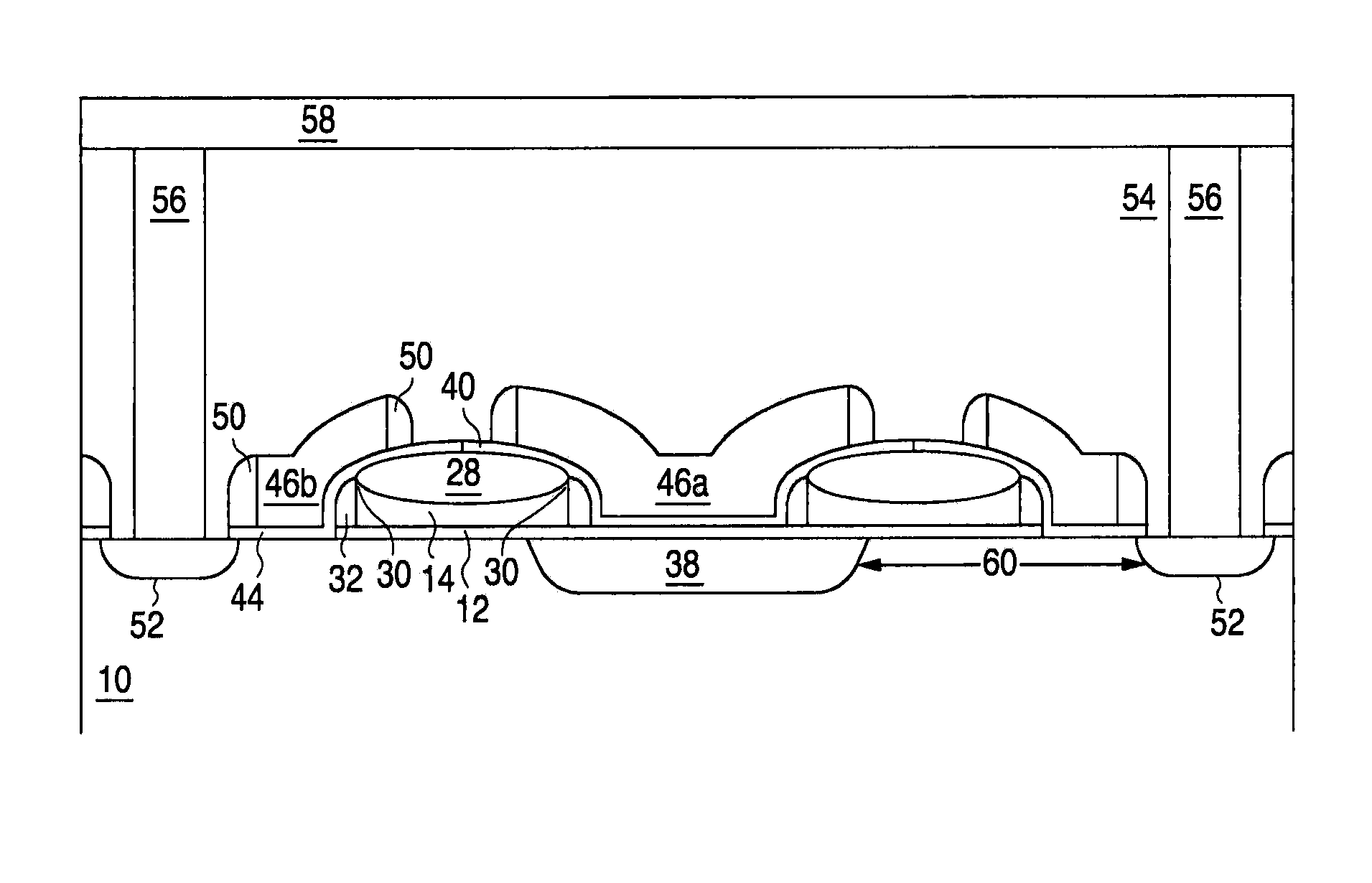
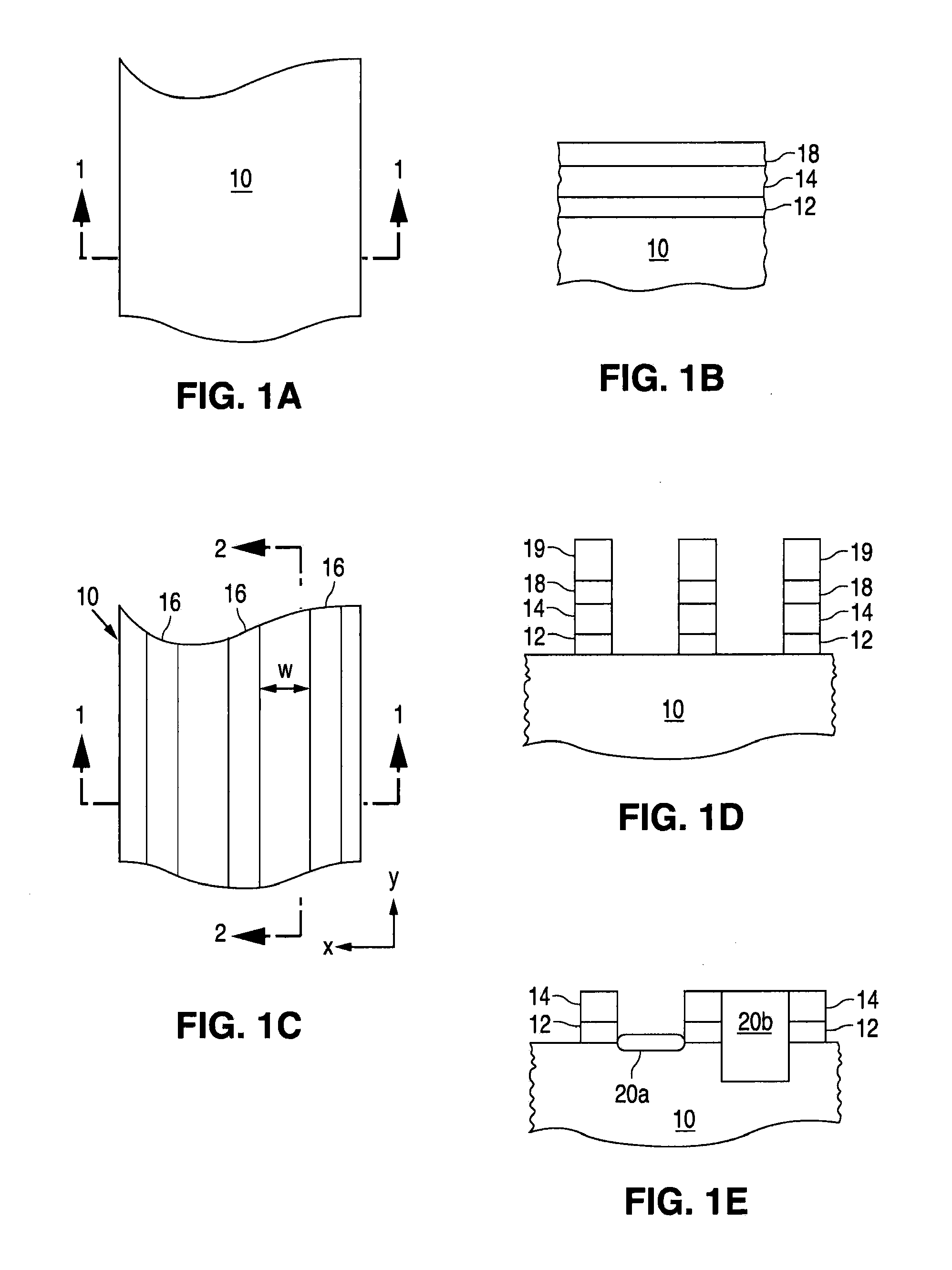
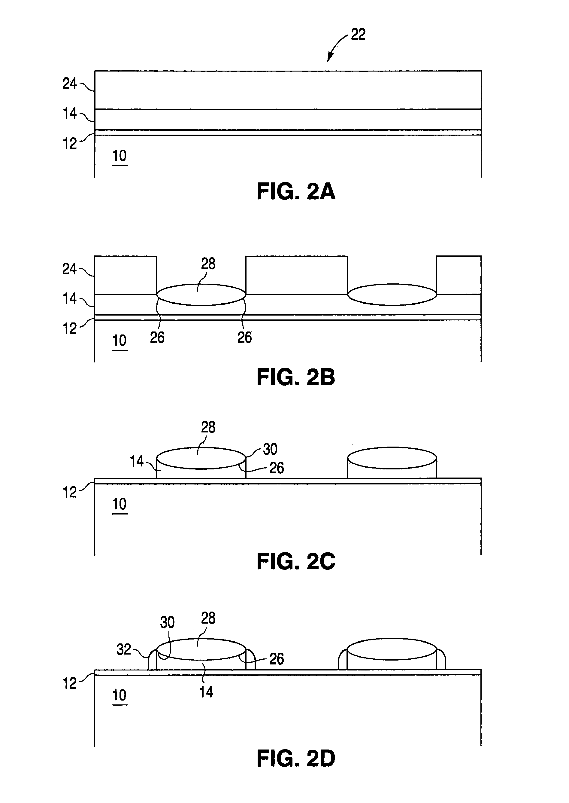
[0020]Referring to FIG. 1A there is shown a top plan view of a semiconductor substrate 10, which is preferably of P type and is well known in the art. A first layer of insulation material 12, ...


PUM


Abstract

A memory device, and method of making and operating the same, including a substrate of semiconductor material of a first conductivity type, first and second spaced apart regions in the substrate of a second conductivity type with a channel region therebetween, an electrically conductive floating gate having a first portion disposed over and insulated from the channel region and a second portion disposed over and insulated from the first region and including a sharpened edge, an electrically conductive P / E gate having a first portion disposed over and insulated from the first region and a second portion extending up and over the floating gate second portion and insulated therefrom by a first layer of insulation material, and an electrically conductive select gate having a first portion disposed laterally adjacent to the floating gate and disposed over and insulated from the channel region.

Description

TECHNICAL FIELD[0001]The present invention relates to a self-aligned method of forming a semiconductor memory array of floating gate memory cells of the split gate type. The present invention also relates to a semiconductor memory array of floating gate memory cells of the foregoing type.BACKGROUND OF THE INVENTION[0002]Non-volatile semiconductor memory cells using a floating gate to store charges thereon and memory arrays of such non-volatile memory cells formed in a semiconductor substrate are well known in the art. Typically, such floating gate memory cells have been of the split gate type, or stacked gate type, or a combination thereof, using a control gate to program, erase and read the memory cell.[0003]Two major issues are often implicated as memory cell dimensions are scaled down. First, the resistance in the source line increases with smaller memory cell dimensions, and a higher resistance suppresses the desirable cell current during a read event. Second, smaller memory cel...

Claims


Application Information

Patent Timeline
Patent Type & Authority Patents(United States)
IPC IPC(8): H01L29/788G11C16/04H01L21/8247H01L27/115H01L29/423
CPCH01L27/115H01L27/11521H01L29/42328H01L29/7885G11C16/0433H10B69/00H10B41/30
Inventor KLINGER, PAVELLEVI, AMITAY
Owner SILICON STORAGE TECHNOLOGY
Why Eureka
Try Eureka