

Semiconductor integrated circuit designing method and program
a technology of integrated circuits and integrated circuits, applied in the direction of cad circuit design, program control, instruments, etc., can solve the problems of inability to improve the yield of loose design rules, the inability to shorten the inability to solve the inability to reduce the number of wirings derived from replacement with a first cell, so as to reduce the time required for automatic arrangement and connection, the effect of preventing the inability to reduce the number of wiring
- Summary
- Abstract
- Description
- Claims
- Application Information
AI Technical Summary
Benefits of technology
Problems solved by technology
Method used
Image

Examples
first embodiment
[0042]Referring to FIG. 1 to FIG. 13, embodiments of the present invention to be adapted to a semiconductor memory device will be described below. the present invention will be described in conjunction with FIG. 1A to FIG. 5B.
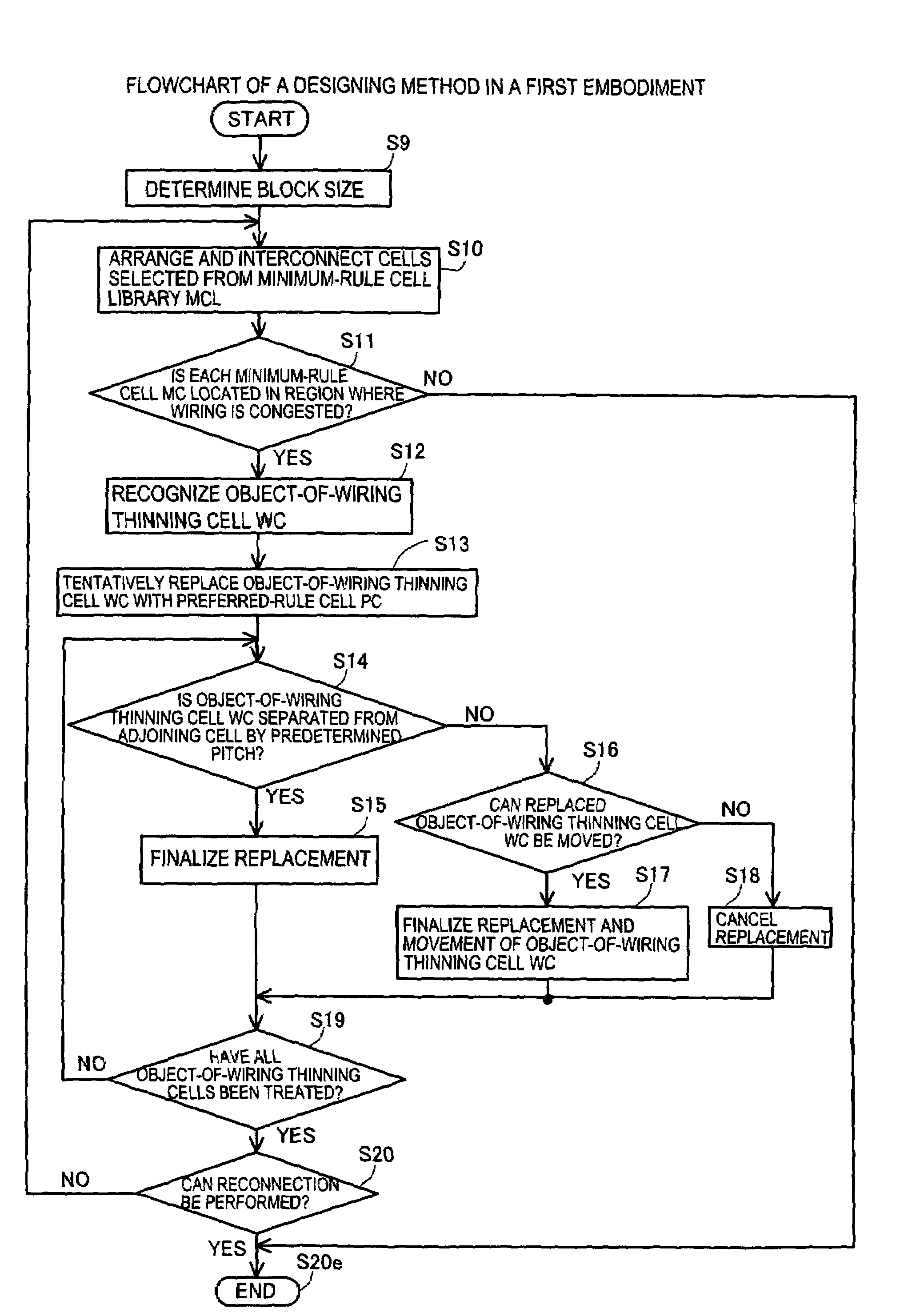
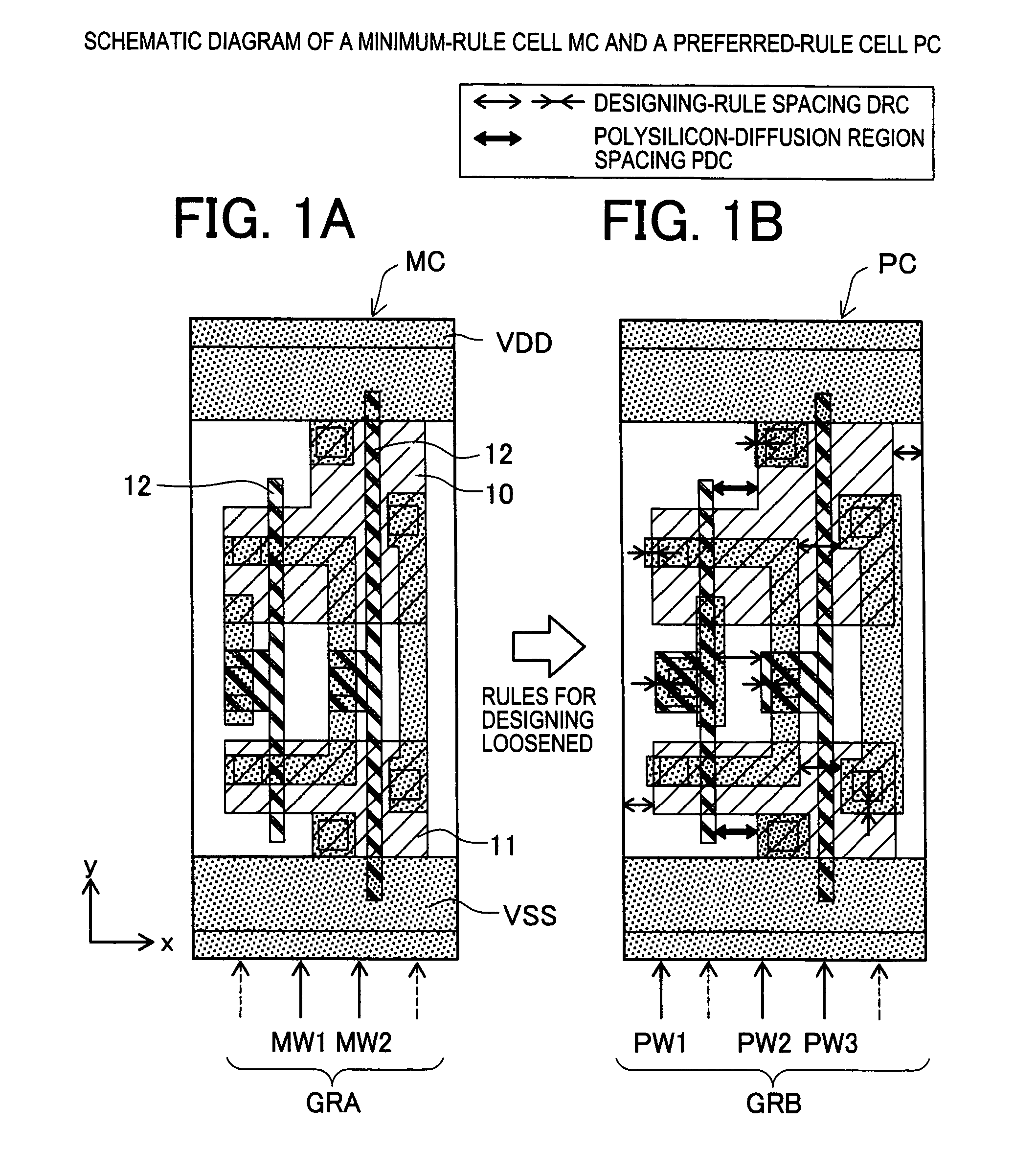
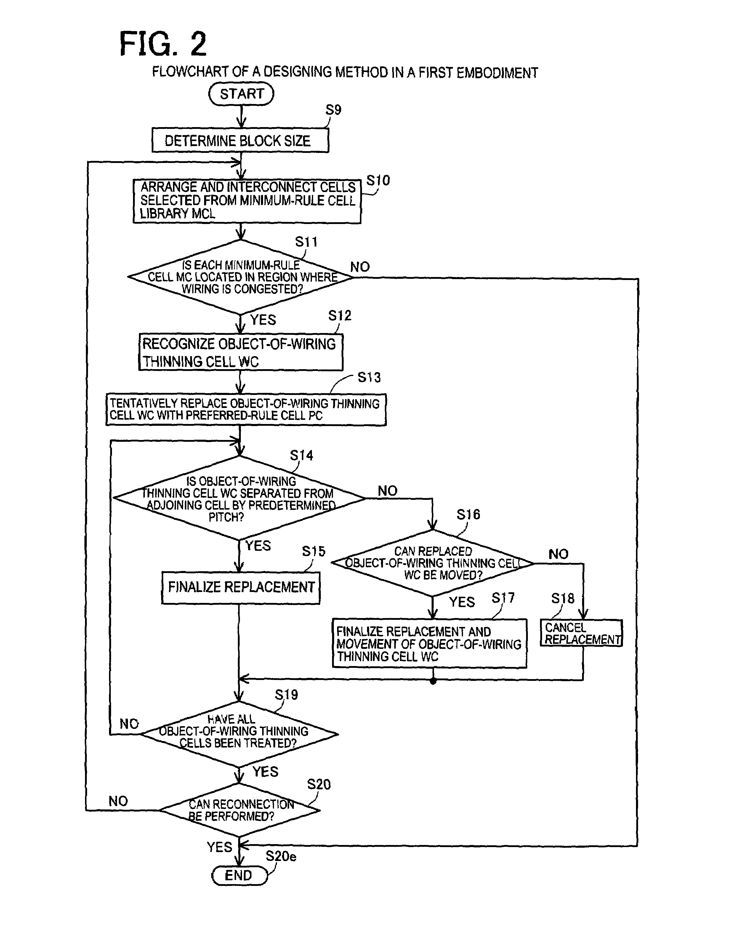
[0043]A semiconductor integrated-circuit device that is a product available in a small lot and in diverse types is requested to be developed for a short period of time and is therefore often designed by an automatic arrangement / connection system including a computer. Among various automatic arrangement / connection methods that are known, a standard cell method is often adopted. According to the standard cell method, the patterns of basic gates or logical circuits whose use frequencies are high are registered as standard cells in a cell library. Based on a netlist concerning a semiconductor integrated-circuit device to be manufactured, the standard cells are arranged and interconnected. Thus, automatic arrangement and designing are completed. The cells have a wir...
second embodiment
[0069]As described above, according to a semiconductor integrated circuit designing method of the second embodiment, when an unconnected state is caused by arranging preferred-rule cells PC, an object-of-movement cell SC is moved in the state of a preferred-rule cell PC or the object-of-movement cell SC is replaced with a minimum-rule cell MC and then moved. Thus, the unconnected state is resolved. Specifically, cells including terminals that should be connected to each other are moved to approach each other and then moved to a region in which wiring is not congested. Thus, a channel is reserved, and the unconnected state is resolved. Moreover, an obstacle cell that hinders connection of terminals that should be connected to each other is moved in order to reserve a channel. Thus, the unconnected state may be resolved. After a preferred-rule cell PC is moved, when it is not separated from an adjoining cell by a predetermined pitch, the preferred-rule cell is replaced with a minimum-...
third embodiment
[0079]As described above, according to a semiconductor integrated circuit designing method of the third embodiment, the freedom in moving cells is ensured, calculation employed in automatic arrangement and connection reliably converges, an unconnected state does not occur, and a free region devoid of a cell is utilized most effectively. A cell ratio can be optimized in order to maximize the number of preferred-rule cells PC. A target cell use rate UR is used as an index for optimizing the cell ratio, namely, the cell ratio is determined so that it will meet the target cell use rate UR. Thus, an optimal cell ratio can be determined quickly and readily. Since the cell ratio is optimized, while occurrence of an unconnected state is prevented, improvement of a yield attributable to the fact that the rules for designing are loosened because of the use of preferred-rule cells PC, and reduction in the total time required for automatic arrangement and connection can be maximized.
[0080]A fou...
PUM
 Abstract
Description
Claims
Application Information