
Bidirectional high voltage switching device and energy recovery circuit having the same

a high-voltage switching device and energy recovery circuit technology, applied in the direction of gas-blowing apparatus, pulse generator, pulse technique, etc., can solve the problems of inconvenient use of fet 100, inappropriate fet, inappropriate fet, etc., and achieve the effect of reducing the amount of energy consumed and efficiently driving

Inactive Publication Date: 2008-01-15
SAMSUNG ELECTRONICS CO LTD
View PDF16 Cites 11 Cited by
  • Summary
  • Abstract
  • Description
  • Claims
  • Application Information

AI Technical Summary

Benefits of technology

The present patent provides a bi-directional high voltage switching device that can conduct current bi-directionally at high voltages and is not affected by parasitic body diodes. It also provides an energy recovery circuit that reduces the amount of energy consumed when charging or discharging a load capacitor, by efficiently driving the bi-directional high voltage switching device. The technical effects of this patent are improved performance and efficiency in high voltage switching and energy recovery applications.

Problems solved by technology

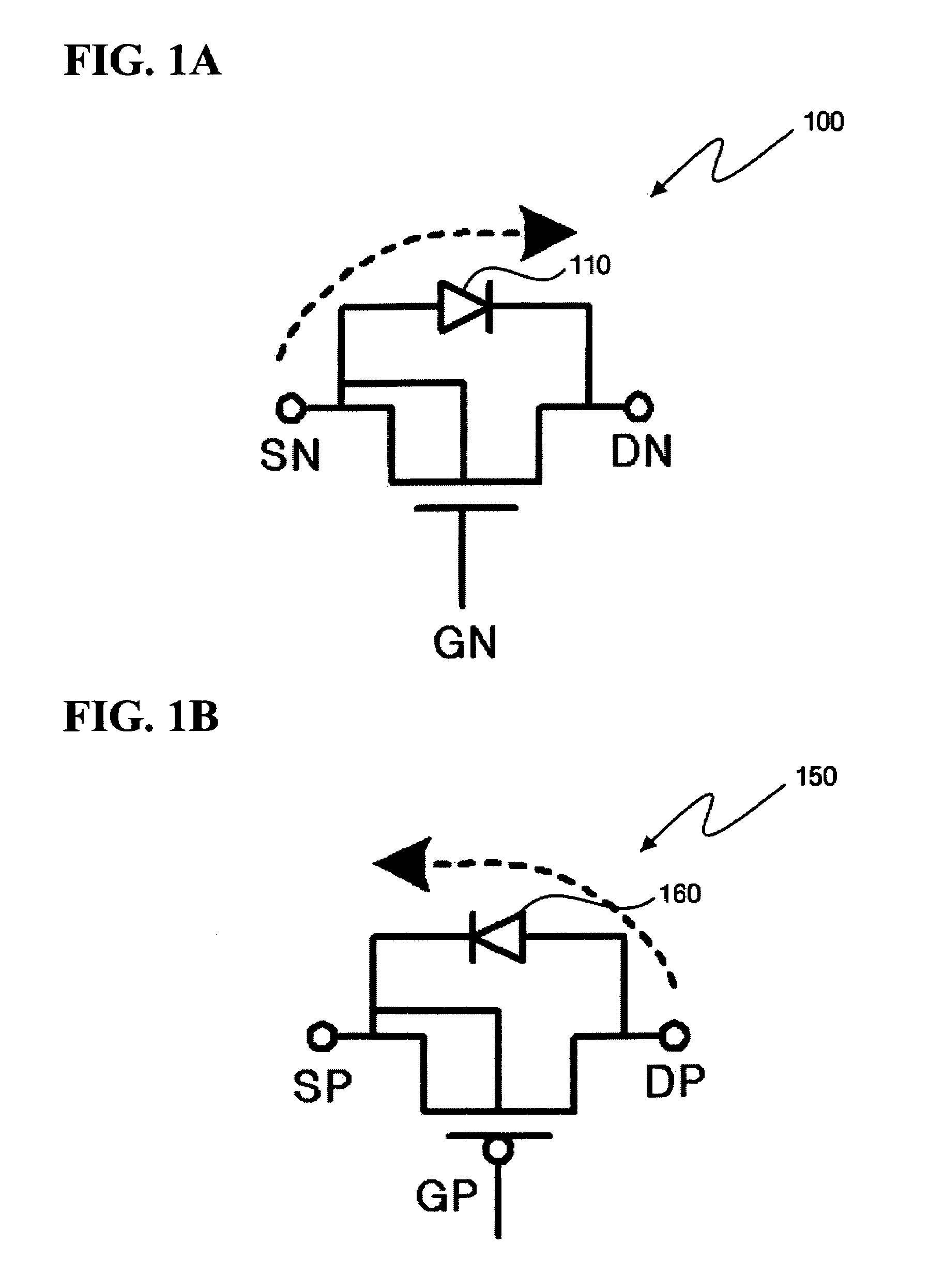
However, a conventional DMOS FET is inappropriate for being used as the bi-directional switching device for the energy recovery circuit because of the following reasons.
Therefore, the conventional N-channel DMOS FET 100 is inappropriate for being used as a bi-directional switching device.
Therefore, the conventional P-channel DMOS FET, like the conventional N-channel DMOS FET, is inappropriate for being used as a bi-directional switching device.

Method used


Image

  • Bidirectional high voltage switching device and energy recovery circuit having the same
  • Bidirectional high voltage switching device and energy recovery circuit having the same
  • Bidirectional high voltage switching device and energy recovery circuit having the same

Examples


Embodiment Construction

[0027]The present disclosure will now be described more fully with reference to the accompanying drawings, in which preferred embodiments of the disclosure are shown. The present disclosure may, however, be embodied in many different forms and should not be construed as being limited to the embodiments set forth herein. Rather, these embodiments are provided so that this disclosure will be thorough and complete, and will fully convey the scope of various embodiments of the disclosure to those skilled in the art. The scope of the invention is defined only by the appended claims. Like reference numerals may refer to like elements throughout this description and the drawings.

[0028]A bi-directional high voltage switching device according to the present disclosure includes an N-channel double diffused metal oxide semiconductor field effect transistor (DMOS FET) and a P-channel DMOS FET, each conducting current bi-directionally, and an energy recovery circuit that reduces the amount of en...


PUM


Abstract

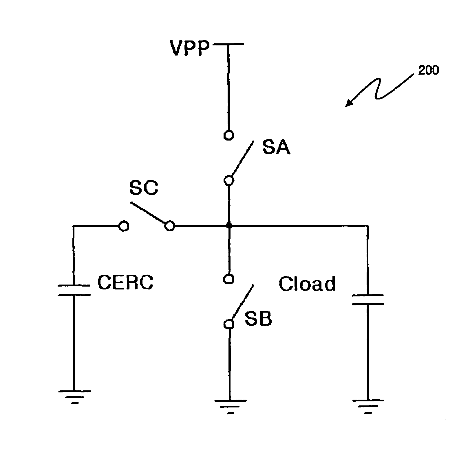
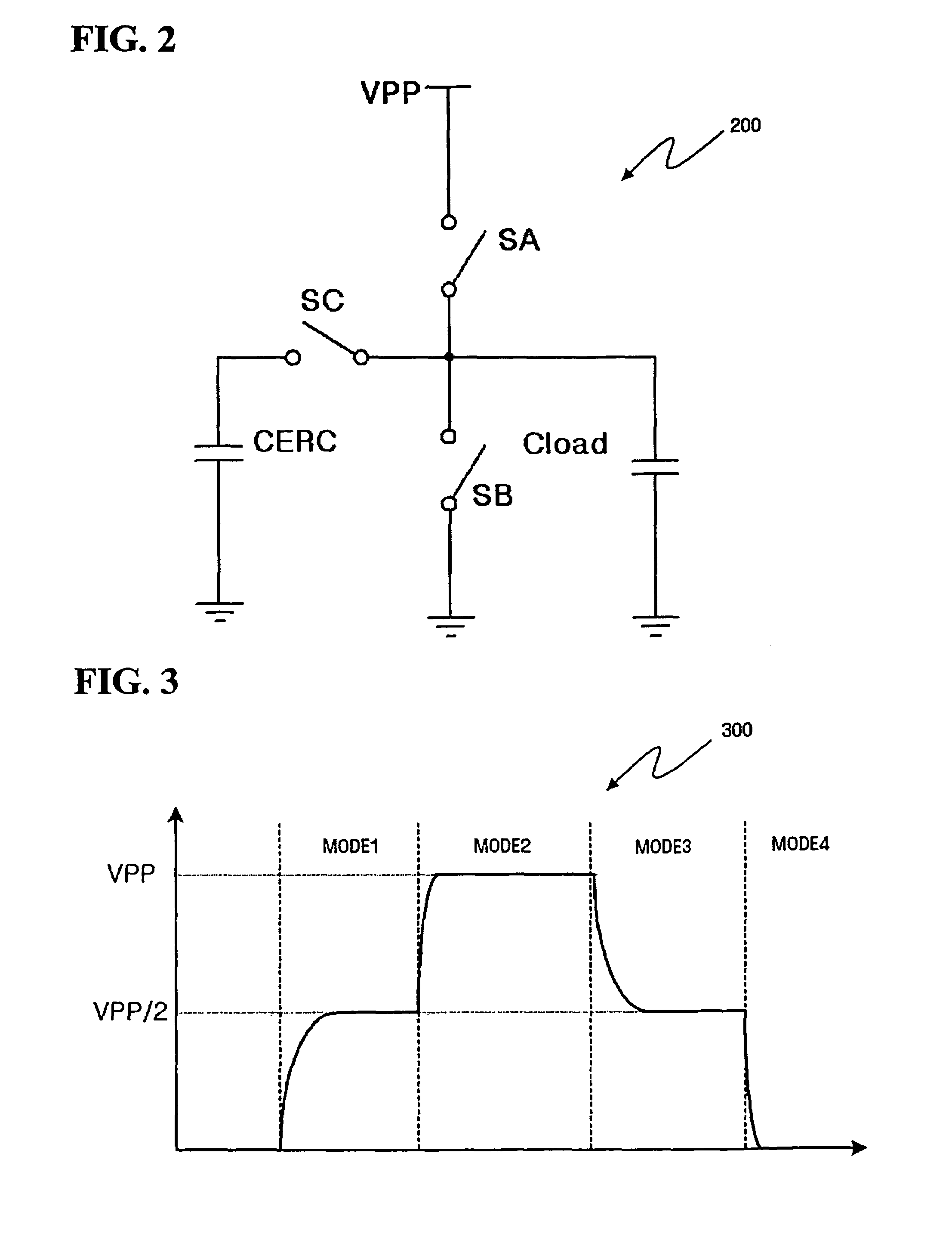
Provided are a bi-directional high voltage switching device that includes an N-channel double diffused metal oxide semiconductor field effect transistor (DMOS FET) and a P-channel DMOS FET, each conducting current bi-directionally, and an energy recovery circuit that reduces the amount of energy consumed when charging or discharging a load capacitor by efficiently driving the bi-directional high voltage switching device; where the N-channel symmetric DMOS FET and the P-channel symmetric DMOS FET are connected to each other in parallel; and the energy recovery circuit includes a pull-up device, a pull-down device, an energy recovery capacitor, and a bi-directional high voltage switching device.

Description

CROSS-REFERENCE TO RELATED APPLICATION[0001]This application claims foreign priority under 35 U.S.C. § 119 to Korean Patent Application No. 10-2004-0004703, filed on Jan. 26, 2004, in the Korean Intellectual Property Office, the disclosure of which is incorporated herein by reference in its entirety.BACKGROUND OF THE INVENTION[0002]1. Field of the Invention[0003]The present disclosure relates to switching devices and energy recovery circuits having the same, and more particularly, to a bi-directional high voltage switching device and an energy recovery circuit that reduces the amount of energy consumed when charging or discharging a load capacitor by efficiently driving the bi-directional high voltage switching device.[0004]2. Description of the Related Art[0005]In order for an energy recovery circuit to make efficient use of energy when using a high voltage as a power supply voltage, the energy recovery circuit additionally includes an energy recovery capacitor that charges a load ...

Claims


Application Information

Patent Timeline
Patent Type & Authority Patents(United States)
IPC IPC(8): H03B1/00H01L21/8238H01L21/822H01L27/04H01L27/07H01L27/092H01L29/10H01L29/78H03K17/687
CPCH01L27/0727H01L29/1033H03K17/6874H01L29/7833H03K17/6872H01L29/1079F41B15/022F41H9/04
Inventor CHO, YOON-JAYSON, IL-HUNBYEON, JAE-IL
Owner SAMSUNG ELECTRONICS CO LTD
Learn More