
Method of generating cell library data for large scale integrated circuits

a technology of integrated circuits and cell libraries, applied in the direction of detecting faulty computer hardware, error detection/correction, instruments, etc., can solve the problems of inapplicability to miniaturized mos transistors, inability to precisely extract resistance values using conventional methods of source and drain resistance extraction, etc., to achieve accurate input-output characteristics and accurate extraction of resistance values

Inactive Publication Date: 2008-01-15
SOCIONEXT INC
View PDF7 Cites 20 Cited by
  • Summary
  • Abstract
  • Description
  • Claims
  • Application Information

AI Technical Summary

Benefits of technology

[0010]It is therefore an object of the present invention to provide a cell library data generating method which can precisely extract source and drain resistance values for miniaturized MOS transistors and generate library data that includes more precise input-output characteristics.
[0012]According to the foregoing first aspect of the invention, when determining the input-output characteristic for a cell constructed of interconnected MOS transistors having source and drain regions with metal silicided surfaces, resistance value characteristics corresponding to the surface areas of the source and drain regions that is particular to miniaturized MOS transistors are used, thereby enabling the accurate extraction of resistance values for miniaturized MOS transistors and making it possible to generate more precise input-output characteristics.

Problems solved by technology

Over the past few years, MOS devices for integrated circuits have been steadily getting smaller.
With the continuing miniaturization of MOS devices, it has become impossible to precisely extract resistance values using conventional methods of extracting source and drain resistances.
However, we have found that such a rule is not applicable to miniaturized MOS transistors.

Method used


Image

  • Method of generating cell library data for large scale integrated circuits
  • Method of generating cell library data for large scale integrated circuits
  • Method of generating cell library data for large scale integrated circuits

Examples


Embodiment Construction

[0025]Embodiments of the invention are described below in conjunction with the attached diagrams. It is to be understood, however, that the technical scope of the invention is not limited by these embodiments, but is limited only by the appended claims and equivalents thereof.

[0026]First, in connection with the description of these embodiments, information included within the library data, such as input-output characteristics, is described here for one example of a cell.

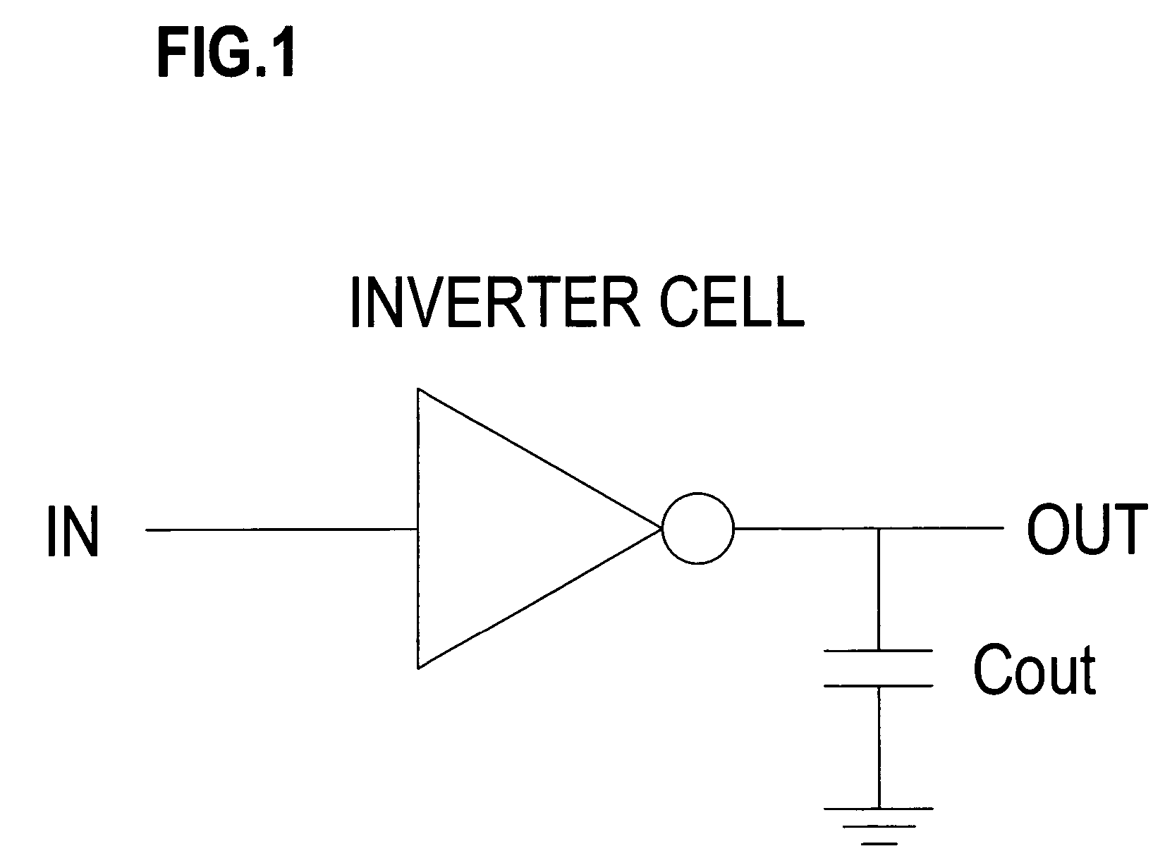
[0027]FIG. 1 is a diagram showing one example of a cell in these embodiments of the invention. This cell is an inverter gate having an input terminal IN and an output terminal OUT. An output load capacitance Cout is connected to the output OUT. The cell has an output signal characteristic for a given input signal, which characteristic is dependent on the ability to drive the transistors making up the inverter gate and the size of the output load capacitance Cout.

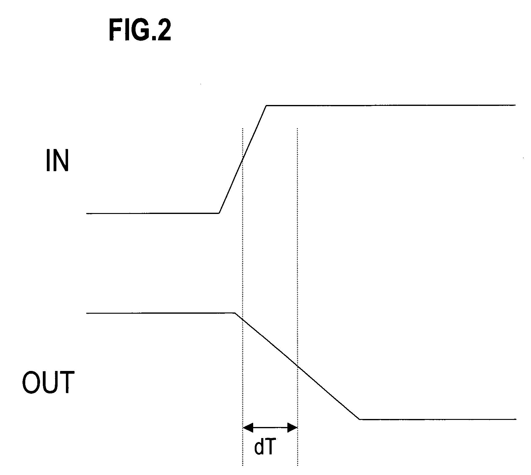
[0028]FIG. 2 is a diagram showing an example of the inp...


PUM


Abstract

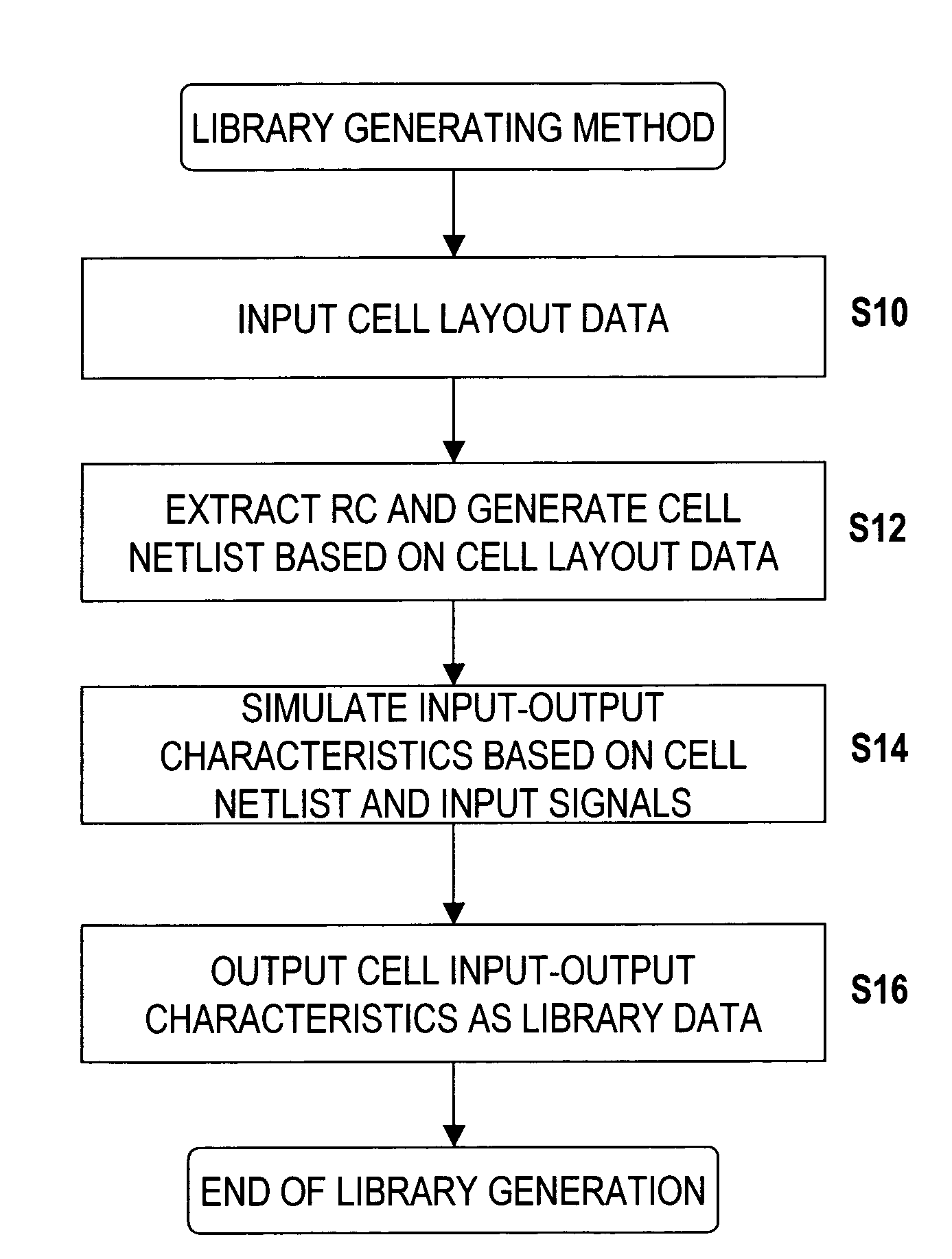
A method of generating library data for a cell constructed of interconnected MOS transistors, includes a resistance extraction step which extracts source and drain resistances according to source and drain region surface areas by using a resistance calculating formula or referring to a resistance extraction reference file which, when the source and drain regions have a first surface area region, treats the source and drain resistances as resistance values depending on the surface areas, and when the source and drain regions have a second surface area region larger than the first surface area region, treats the source and drain resistances as fixed resistance values; and a simulation step which generates an input-output characteristic for the cell from a netlist containing a MOS transistor model that includes the extracted source resistances and drain resistances and connection information for the model, and from input signals.

Description

CROSS-REFERENCE TO RELATED APPLICATIONS[0001]This application is based upon and claims the benefit of priority from the prior Japanese Patent Application No. 2005-88040, filed in Mar. 25, 2005, the entire contents of which are incorporated herein by reference.BACKGROUND OF THE INVENTION[0002]1. Field of the Invention[0003]The present invention relates to a method of generating cell library data for large scale integrated circuits, and more particularly to a cell library data generating method that can very precisely extract the source-drain resistances of the miniaturized MOS transistors making up the cell and very precisely generate cell input-output characteristics.[0004]2. Description of the Related Art[0005]Application-specific integrated circuits (ASIC) are designed using multiple types of cells that are registered in a library. Each cell is composed of a single MOS transistor or a combination of multiple MOS transistors, and has a specific function (e.g., inverter, NAND, NOR, ...

Claims


Application Information

Patent Timeline
Patent Type & Authority Patents(United States)
IPC IPC(8): G06F17/50
CPCG06F17/5036G06F30/367
Inventor MUKAIHIRA, KAZUNOBU
Owner SOCIONEXT INC
Learn More