Process for manufacturing a triaxial piezoresistive accelerometer and relative pressure-monitoring device

a technology of accelerometer and relative pressure, which is applied in the direction of acceleration measurement in multiple dimensions, acceleration measurement using interia forces, tyre measurement, etc., can solve the problems of unbalancing the wheatstone bridge, cumbersome production process, and cumbersome pressure monitoring device, etc., to achieve simple and inexpensive manufacturing, simple integration

Active Publication Date: 2008-01-29
STMICROELECTRONICS SRL
View PDF8 Cites 36 Cited by
  • Summary
  • Abstract
  • Description
  • Claims
  • Application Information

AI Technical Summary

Benefits of technology

[0014]One embodiment of the present invention provides an accelerometer overcoming the aforesaid disadvantages and problems, and in particular simple and inexpensive to manufacture, and simple to integrate within a pressure-monitoring device, in particular for automotive applications.

Problems solved by technology

Consequently, the pressure-monitoring device is currently cumbersome (around 10 mm in size) and somewhat complex to produce.
Due to this deformation, the piezoresistive elements 6 vary their resistivity, so unbalancing the Wheatstone bridge.
The accelerometer 1 described, even though it is certainly more compact than wake-up systems of a mechanical type, has in any case large dimensions on account of the need to carry out a bonding of three different layers (two layers of silicon and one layer of glass) and on account of the presence of a ceramic package, and entails a manufacturing process that is somewhat complex and costly.
Furthermore, the accelerometer 1 cannot be readily integrated with the electronic read circuit.
These disadvantages are particularly evident as regards the considered automotive applications, wherein low cost and simplicity of production are a constraint in the choice of the components to be used.

Method used


Image

  • Process for manufacturing a triaxial piezoresistive accelerometer and relative pressure-monitoring device
  • Process for manufacturing a triaxial piezoresistive accelerometer and relative pressure-monitoring device
  • Process for manufacturing a triaxial piezoresistive accelerometer and relative pressure-monitoring device

Examples


Embodiment Construction

[0029]Hereinafter an embodiment is described of a manufacturing process of a triaxial piezoresistive accelerometer of semiconductor material. The manufacturing process is based upon the process described in EP-A-1 324 382, for manufacturing a SOI wafer, and on the process described in European patent application No. 04 425 197.3 filed in the name of the present applicant on 19 Mar. 2004, for manufacturing a pressure sensor.

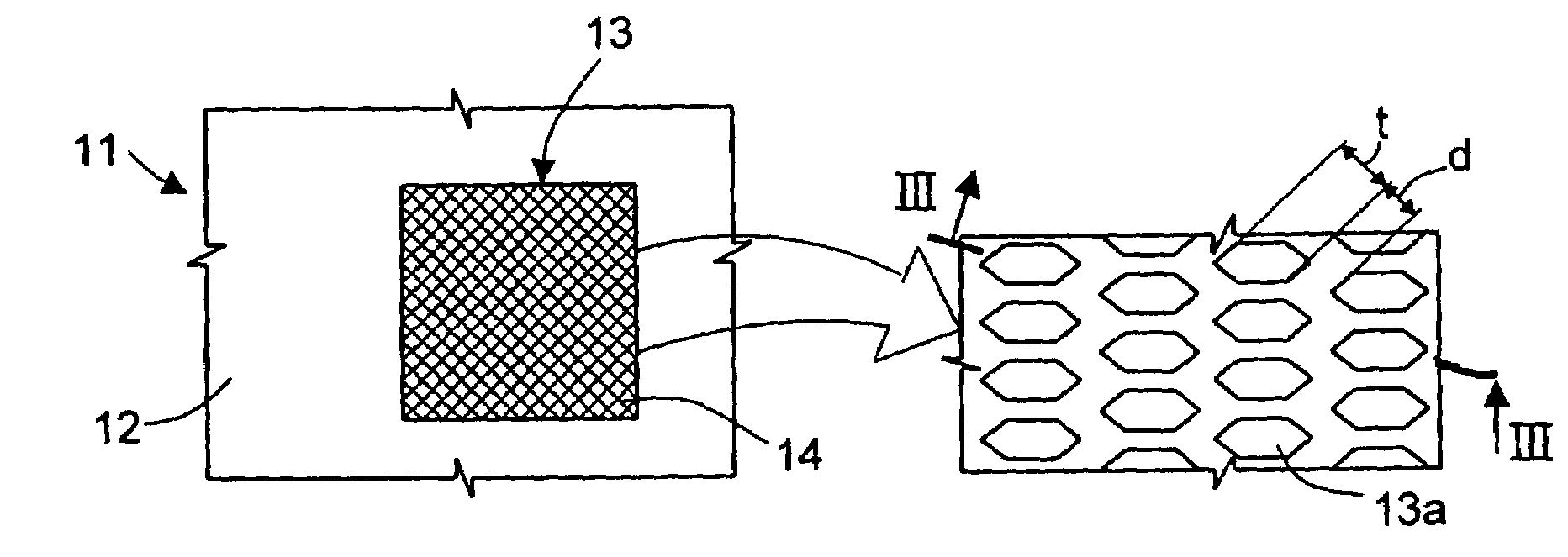
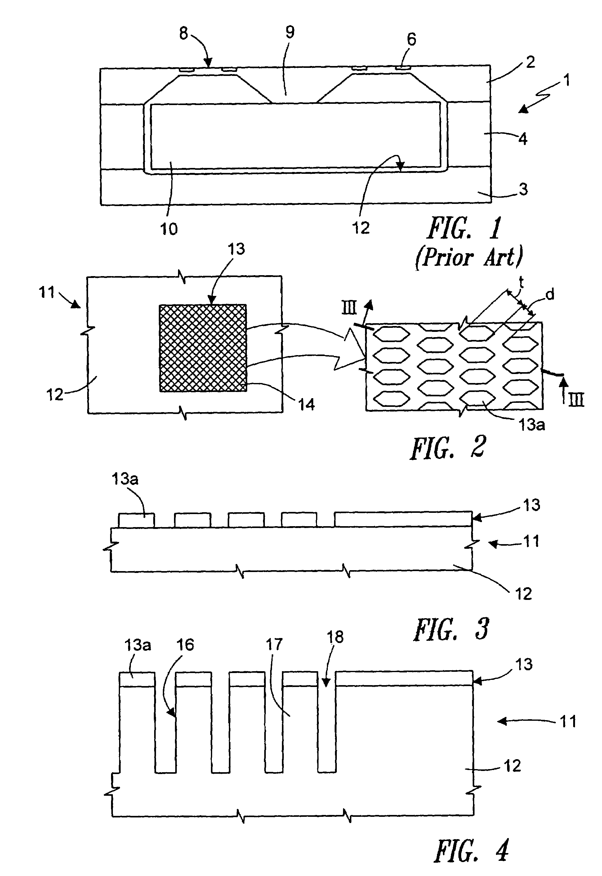
[0030]FIG. 2 shows a wafer 11 of semiconductor material, for example monocrystalline silicon, comprising a substrate 12, for example of N type.

[0031]In an initial step of the manufacturing process, a resist mask 13 is made on the wafer 11 (reference may also be made to the cross-section ofFIG. 3). In detail, the mask 13 has an approximately square area 14 comprising a plurality of hexagonal mask portions 13a that define a honeycomb lattice (as visible in the enlarged detail of FIG. 2). For example, the distance t between opposite sides of the mask portions 13a is ...


PUM


Abstract

A manufacturing process of a semiconductor piezoresistive accelerometer includes the steps of: providing a wafer of semiconductor material; providing a membrane in the wafer over a cavity; rigidly coupling an inertial mass to the membrane; and providing, in the wafer, piezoresistive transduction elements, that are sensitive to strains of the membrane and generate corresponding electrical signals. The step of coupling is carried out by forming the inertial mass on top of a surface of the membrane opposite to the cavity. The accelerometer is advantageously used in a device for monitoring the pressure of a tire of a vehicle.

Description

BACKGROUND OF THE INVENTION[0001]1. Field of the Invention[0002]The present invention relates to a process for manufacturing a triaxial piezoresistive accelerometer and the relative pressure-monitoring device, in particular a device for monitoring the pressure of the tires of a motor vehicle, to which the ensuing description will make explicit reference, without any loss of generality.[0003]2. Description of the Related Art[0004]As known, in the automotive field there is an increasing use of devices for monitoring the pressure of tires (generally known as tire-pressure monitoring systems—TPMSs), which are designed to supply a timely communication, to the electronic control unit of the vehicle, of any fault or deviation with respect to the correct values of operation. These monitoring devices generally comprise a pressure sensor installed on the inner surface of the tire and designed to monitor its state of inflation; an appropriate electronic circuit, which reads the data provided b...

Claims


Application Information

Patent Timeline
Patent Type & Authority Patents(United States)
IPC IPC(8): G01P15/00G01P15/18
CPCG01P15/0802G01P15/123G01P15/18G01P2015/084
Inventor COMBI, CHANTALBALDO, LORENZOFARALLI, DINOVILLA, FLAVIO FRANCESCO
Owner STMICROELECTRONICS SRL
Why Eureka
Try Eureka