Methods and apparatus for monitoring a process in a plasma processing system by measuring self-bias voltage

a plasma processing system and self-bias voltage technology, applied in the direction of individual semiconductor device testing, semiconductor/solid-state device testing/measurement, instruments, etc., can solve the problem of increasing the heat transfer rate, difficult to determine exactly when the process conditions change beyond established parameters, and contamination, in particular, tends to present a substantial problem

Active Publication Date: 2008-01-29
LAM RES CORP
View PDF15 Cites 30 Cited by
  • Summary
  • Abstract
  • Description
  • Claims
  • Application Information

AI Technical Summary

Benefits of technology

[0070]Advantages of the invention include methods and apparatus for monitoring a process in a plasma processing system by measuring self-bias voltage. Additional advantages include the use of a substantially reliable signal that can be used for diagnostics or monitoring purposes.

Problems solved by technology

That is, increasing helium pressure subsequently also increases the heat transfer rate.
However, in these and other plasma processes, it is often difficult to determine exactly when process conditions change beyond established parameters.
Contamination, in particular, tends to present a substantial problem.
Since fully removing deposits may be time consuming, a plasma processing system chamber is generally only substantially cleaned when the particle contamination levels reach unacceptable levels, when the plasma processing system must be opened to replace a consumable structure (e.g., edge ring, etc.), or as part of scheduled preventive maintenance (PM).
Likewise, hardware deterioration also tends to be problematic.
As plasma chamber components are exposed to the plasma, they themselves may become damaged, altering mechanical and electrical characteristics, as well as producing contaminants.
In fact, the cleaning process itself may damage the components, as with the electrostatic chuck (chuck) during waferless auto clean or (WAC).
Yet, there is generally no effective way to determine if a plasma process has moved outside of established parameters in-situ, without first initially processing and then subsequently testing partially manufacturing substrates.
If the test determines that the substrate does not meet the established specification, the entire batch of substrates may need to be destroyed.
However, creating an empirical model may be problematic.
However, even a loosely correlated (and hence weakly predictive) model is difficult to obtain since repetition of the plasma process itself may effect of the electrical characteristics of plasma processing system components.

Method used


Image

  • Methods and apparatus for monitoring a process in a plasma processing system by measuring self-bias voltage
  • Methods and apparatus for monitoring a process in a plasma processing system by measuring self-bias voltage
  • Methods and apparatus for monitoring a process in a plasma processing system by measuring self-bias voltage

Examples


Embodiment Construction

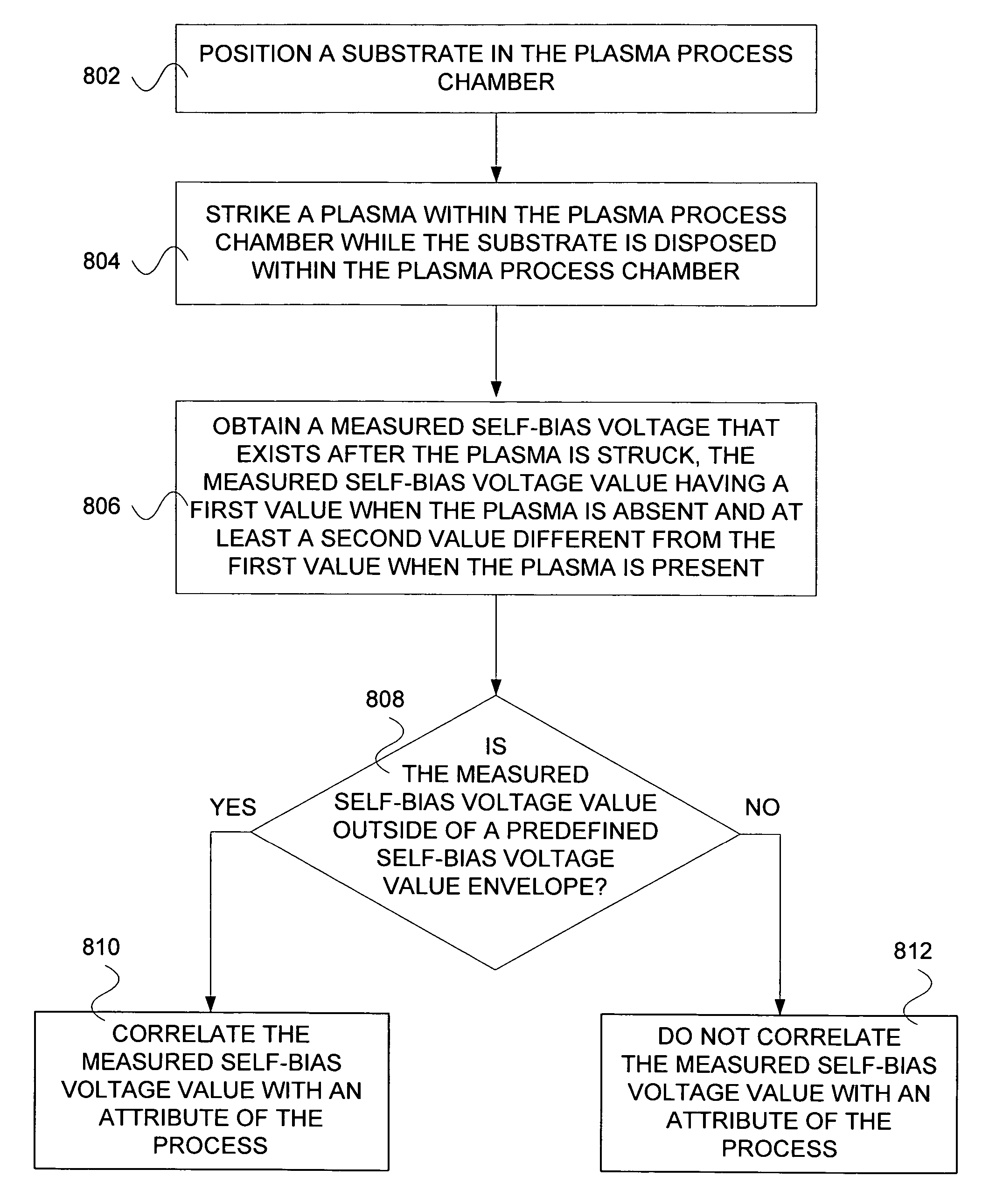
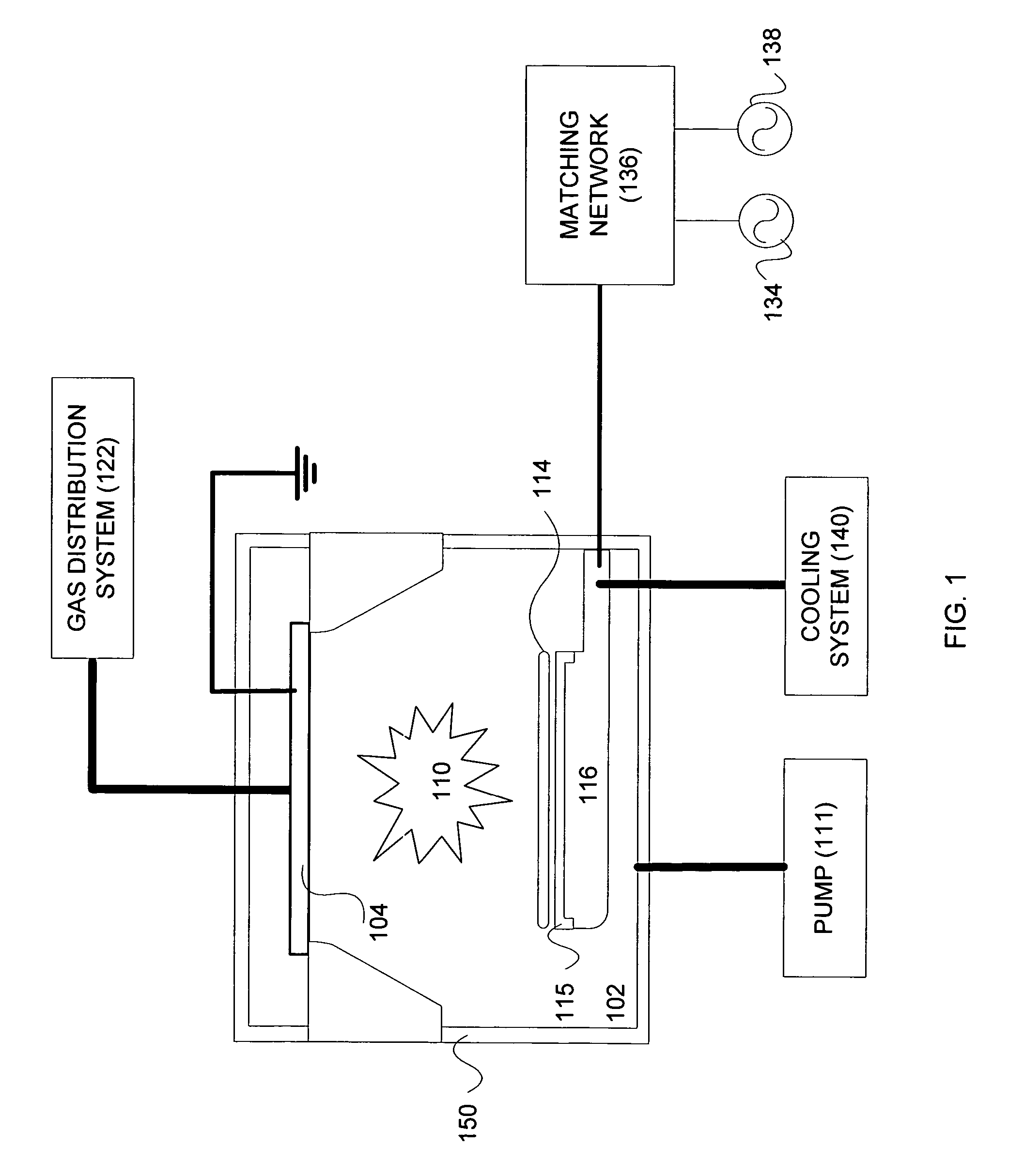
[0027]The present invention will now be described in detail with reference to a few preferred embodiments thereof as illustrated in the accompanying drawings. In the following description, numerous specific details are set forth in order to provide a thorough understanding of the present invention. It will be apparent, however, to one skilled in the art, that the present invention may be practiced without some or all of these specific details. In other instances, well known process steps and / or structures have not been described in detail in order to not unnecessarily obscure the present invention.

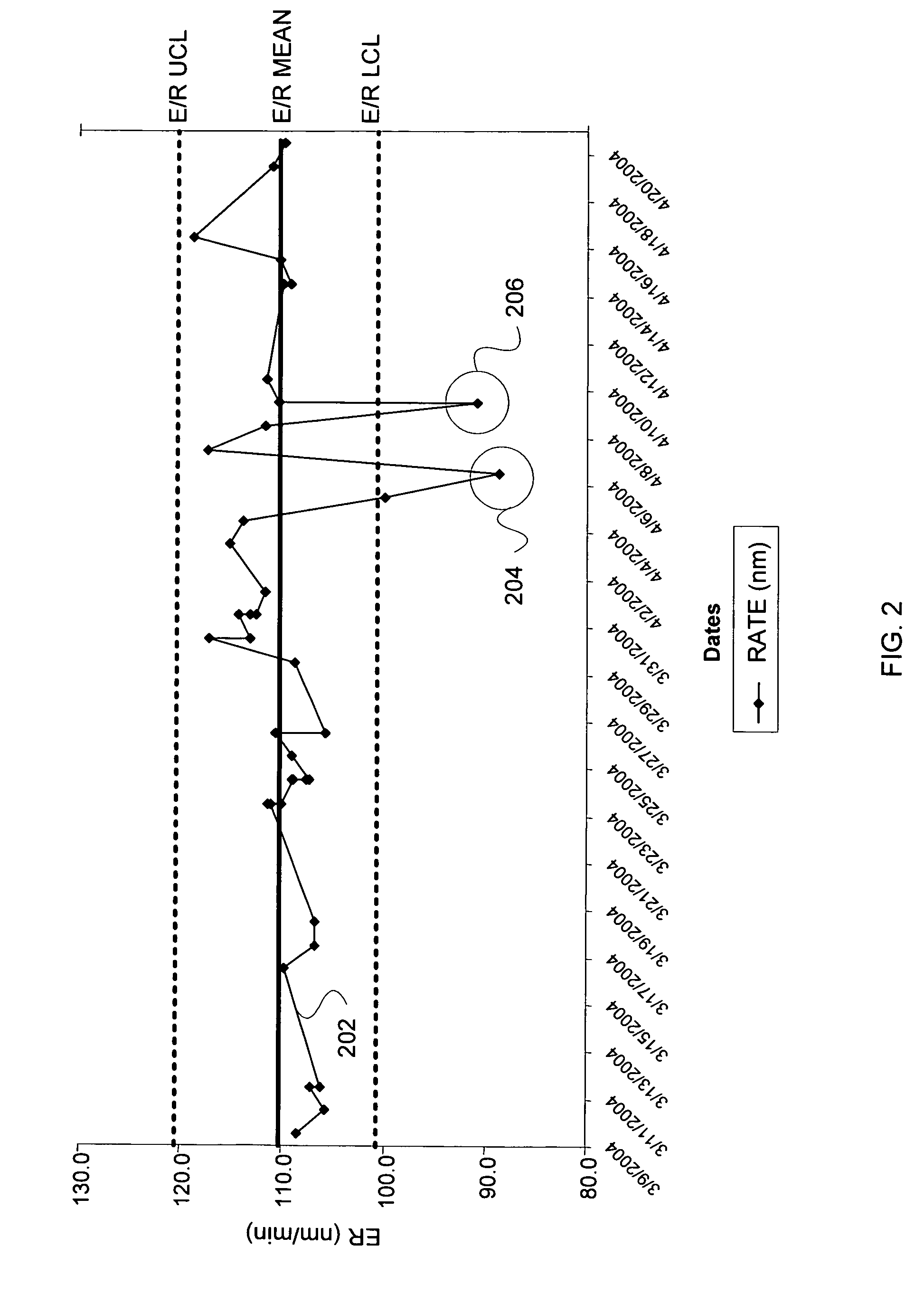
[0028]While not wishing to be bound by theory, it is believed by the inventor herein that a substantially easy-to-measure plasma parameter excursion can be correlated to a substantially difficult-to-measure substrate attribute excursion. Generally, an excursion represents a data point that is outside of an established statistical range or a value envelope. That is, an excursion may be a da...


PUM

PropertyMeasurementUnit
RF frequencyaaaaaaaaaa

Abstract

A method for in-situ monitoring a process in a plasma processing system having a plasma processing chamber is disclosed. The method includes positioning a substrate in the plasma processing chamber. The method also includes striking a plasma within the plasma processing chamber while the substrate is disposed within the plasma processing chamber. The method further includes obtaining a measured self-bias voltage that exists after the plasma is struck, the measured self-bias voltage value having a first value when the plasma is absent and at least a second value different from the first value when the plasma is present. The method also includes correlating the measured self-bias voltage value with an attribute of the process, if the measured self-bias voltage value is outside of a predefined self-bias voltage value envelope.

Description

BACKGROUND OF THE INVENTION[0001]The present invention relates in general to substrate manufacturing technologies and in particular to methods and apparatus for monitoring a process in a plasma processing system by measuring self-bias voltage.[0002]In the processing of a substrate, e.g., a semiconductor substrate or a glass panel such as one used in flat panel display manufacturing, plasma is often employed. As part of the processing of a substrate for example, the substrate is divided into a plurality of dies, or rectangular areas, each of which will become an integrated circuit. The substrate is then processed in a series of steps in which materials are selectively removed (etching) and deposited (deposition) in order to form electrical components thereon.[0003]In an exemplary plasma process, a substrate is coated with a thin film of hardened emulsion (i.e., such as a photoresist mask) prior to etching. Areas of the hardened emulsion are then selectively removed, causing component...

Claims


Application Information

Patent Timeline
Patent Type & Authority Patents(United States)
IPC IPC(8): G01R31/00
CPCH01J37/32935H01L21/30H01L21/306
Inventor GUINEY, TIMOTHY J.ANNAPRAGADA, RAODESHMUKH, SUBHASHCHENG, CHIA CHENG
Owner LAM RES CORP
Why Eureka
Try Eureka