AFM-based lithography metrology tool

a lithography metrology and lithography technology, applied in the field of semiconductor manufacturing methods and systems, can solve the problems of time-consuming and labor-intensive stand-alone ol or cd-sem apparatuses, repeated errors or defects, and inability to accurately measure the mechanical properties of the instrument, so as to save precious space and reduce the size

Inactive Publication Date: 2005-09-22
APPLIED MATERIALS INC
View PDF26 Cites 14 Cited by
  • Summary
  • Abstract
  • Description
  • Claims
  • Application Information

AI Technical Summary

Benefits of technology

[0067] As is well known, the space that a typical CD-SEM occupies in the clean room, where the track is situated, is by any standard considerably large. In contrast, the AFM is significantly smaller in size which not only allows to use it in clean room, saving thus precious space, but also enables to use it as a station on the track, which as will be explained below brings about many advantages.

Problems solved by technology

In prior art, the inspection of a batch of wafers during the photolithograpy step has been executed on a sampling bases only, due to the inherent prolonged and cumbersome process of inspection, which necessitates actual removal of the inspection wafer from the track and feeding the wafer to the overlay machine.
Thus, in case of errors or defects, all wafers of the batch exhibited the same problem.
By not inspecting each wafer individually, errors or defects were repeatedly produced.
The handling of samples from the track to the stand-alone OL or CD-SEM apparatus is time consuming and can introduce contamination and mechanical damage due to wafer handling.
The number of available inspection tools per photolithographic station, typically about one OL tool per four photolithographic stations, causes bottleneck situations, which substantially adversely affect throughput.
The introduction of advanced photomasks for subwavelength (beyond 0.25 micron) integrated circuit (IC) manufacturing, reaching the envelope of optical OL capabilities, thus bringing about a substantial decrease of optical image quality, and consequently, rendering the conventional OL tools less and less useful.
The increasingly frequent use of CMP (Chemical Mechanical Planarization—a technique to flatten the surface of the added layers of conductive or insulating materials) induces low-contrast images, which lowers the accuracy of optical OL measurement systems.
This flattening reduces the average height of a layer-line to approach the envelope of optical OL capabilities, thus bringing about a substantial decrease of optical image quality.
It is important to notice that the current trend of even more reduction of average height of layer lines will go beyond the envelope of optical OL capabilities, thus severely limiting the conventional optical OL tools.
Submitting the wafer to vacuum during the CD-SEM inspection is a time consuming step, using complex equipment and setup.
Although both overlay and CD monitoring measurements are similar in the metrology used, there has been no prior art solutions found for using one and the same tool for both tasks.
Moreover, it is not apparent how to go about combining both tasks since traditional CD-SEM and overlay equipment have different requirements (e.g., electron optics and vacuum for CD-SEM and light optics with no vacuum for overlay).
Due to sever space limitations traditional CD-SEM and / or overlay cannot be placed in the track.

Method used


Image

  • AFM-based lithography metrology tool
  • AFM-based lithography metrology tool
  • AFM-based lithography metrology tool

Examples


Embodiment Construction

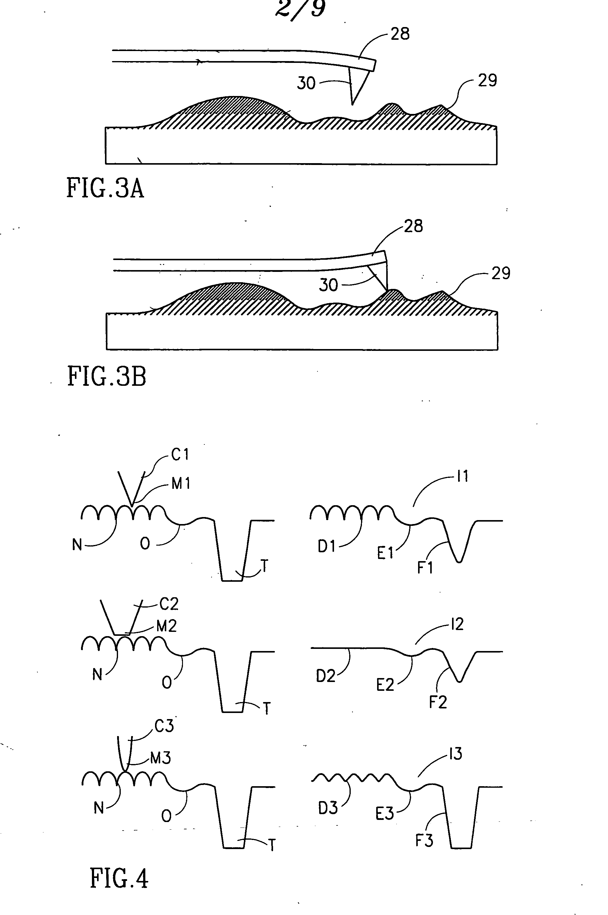
[0095] There follows now a description of usage of a known per se AFM (with reference also to FIG. 3) which, as will be explained briefly below, is utilized in the preferred embodiment of the present invention for OL and / or CD inspection. For technical background about the AFM and related publications referral is made to U.S. Pat. Nos. 4,724,318; 5,189,906; and 5,666,190 [5][6][7], incorporated here by reference.

[0096] Scanning probe microscopy (SPM) refers to several techniques that use the interaction of a microscopic stylus probe 28 with the surface 29 of a sample to measure characteristics of the sample surface at localized points. A fine tip (30) is brought into atomically close contact with a sample surface without actually touching the surface 29. By means of sensing the repulsive force between the stylus probe tip and the surface a signal is generated that is used to keep a constant distance between the tip and the surface. This mode is called Non-Contact Mode A. The force...


PUM

PropertyMeasurementUnit
diameteraaaaaaaaaa
diameteraaaaaaaaaa
forcesaaaaaaaaaa

Abstract

A photolithographic track system and method for semiconductor wafer manufacture having a plurality of stations for receiving a wafer for sequential processing, including a first group of stations for performing at least a part of a photolithography process. A metrology station is provided in a position of the track system after the first group of stations, for determining whether the processed wafer is within tolerance for at least one critical dimension. If not within tolerance, the wafer is moved by the track system to a stripping station for removal of at least one layer and a return to the beginning of the first group of stations for repeating the performance of a photolithography process. Parameters may also be adjusted for purposes of the repeated performance of the process. If within tolerance, the wafer may be moved for further processing, for example, baking or off loading.

Description

FIELD OF THE INVENTION [0001] The present invention relates to a semiconductor manufacturing method and system and more particular to a method and system that includes monitoring and quality control constituents such as overlay (OL) and critical dimension (CD) tools. REFERENCES [0002] There follows a list of references that is referenced in the following description. [0003] 1. http: / / www.sematech.org / public / dict / home.htm [0004] 2. http: / / www.encyclopedia.com / articles / 13734.html [0005] 3. http: / / www.fullman.com / semiconductors / index.html [0006] 4. http: / / www.veeco.com / metrology.html [0007] 5. U.S. Pat. No. 4,724,318 February 1988 Gerd K. Binning [0008] 6. U.S. Pat. No. 5,189,906 March 1993 Elings et al [0009] 7. U.S. Pat. No. 5,666,190 September 1997 Quate and Minne [0010] 8. http: / / www.york.ac.uk / org / esca / tech / afm.html [0011] 9. http: / / home.ee.umanitoba.ca / ˜spm / index.html [0012] 10. http: / / www.topometrix.com / afmodes1.htm [0013] 11. http: / / www.al.com / asm / afmpage.htm [0014] 12. http: / / ...

Claims


Application Information

Patent Timeline
Patent Type & Authority Applications(United States)
IPC IPC(8): G01B5/28G01N23/00G01Q60/24G01Q80/00G03F7/20
CPCG01Q80/00B82Y10/00G03F7/70633G03F7/70625
Inventor DANA, STEPHANEBACH, JOSEPH
Owner APPLIED MATERIALS INC
Why Eureka
Try Eureka