Semiconductor device having an improved voltage controlled oscillator

a technology of voltage control and oscillator, which is applied in the direction of pulse generator, pulse technique, modulation, etc., can solve the problems of deteriorating noise characteristics of the voltage control oscillation circuit, and achieve the effect of reducing the serial resistance component of the variable-capacity element and the resistance component in the horizontal direction between the respective base layers

Active Publication Date: 2008-01-29
MURATA MFG CO LTD
View PDF18 Cites 10 Cited by
  • Summary
  • Abstract
  • Description
  • Claims
  • Application Information

AI Technical Summary

Benefits of technology

[0012]The semiconductor device according to the present invention is composed as described above, and the resistance component in the horizontal direction between respective base layers is decreased. As a result, the serial resistance component of the variable-capacity element is decreased.

Problems solved by technology

Thus, the noise characteristics of the voltage-controlled oscillation circuit is deteriorated.

Method used


Image

  • Semiconductor device having an improved voltage controlled oscillator
  • Semiconductor device having an improved voltage controlled oscillator
  • Semiconductor device having an improved voltage controlled oscillator

Examples


Embodiment Construction

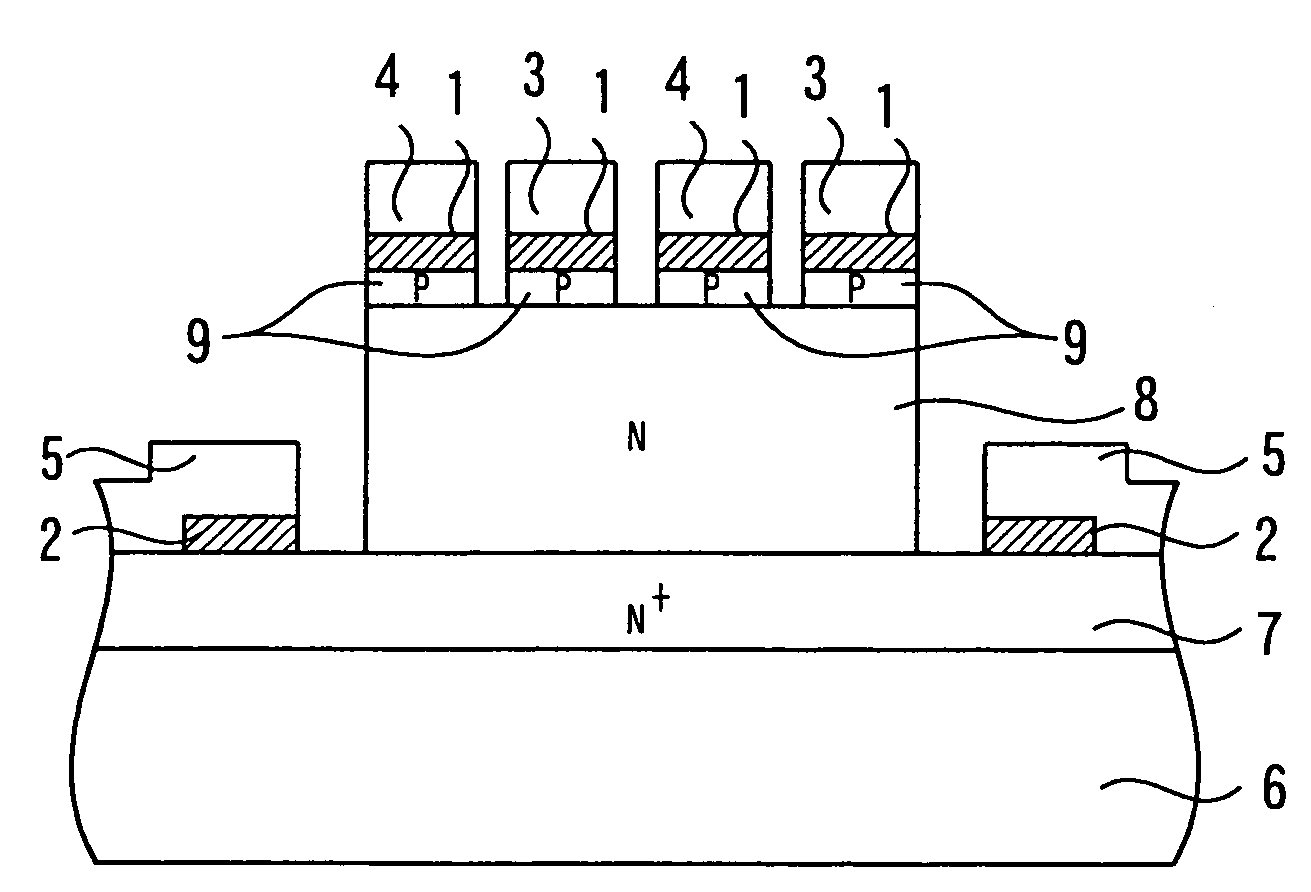
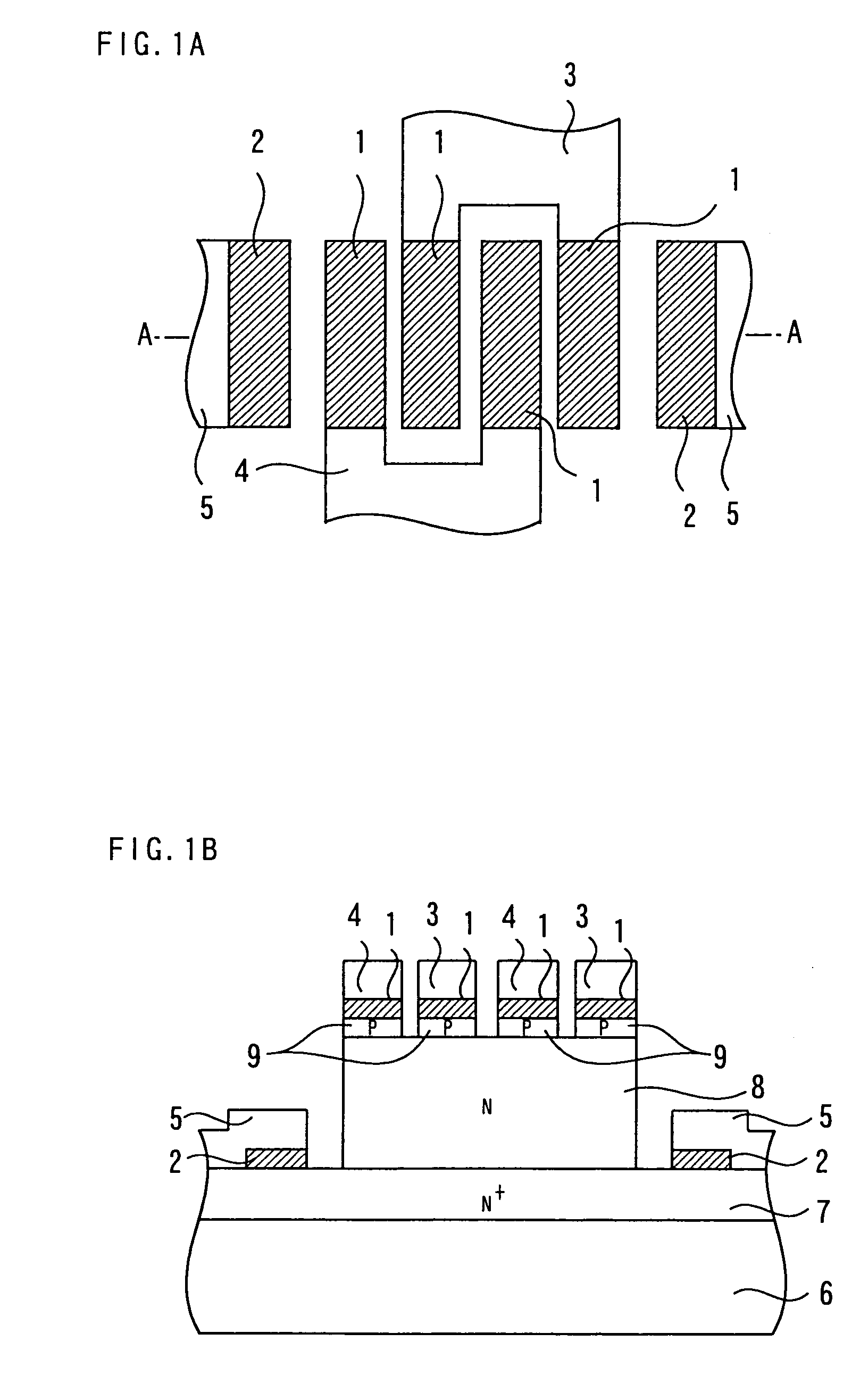
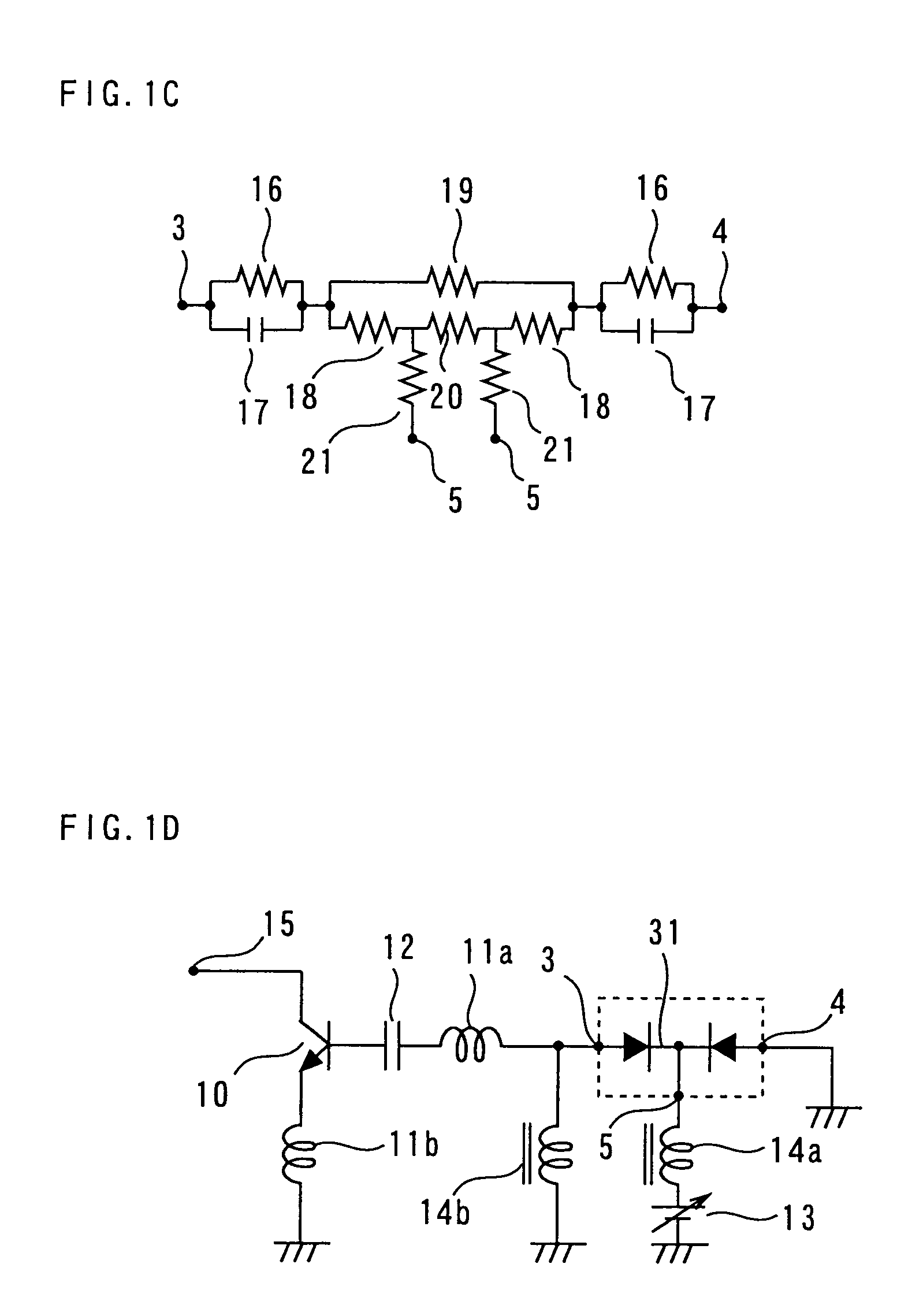
[0024]A preferred embodiment of the present invention will be described below referring to the drawings. FIG. 1A is a plan view showing the constitution of a variable-capacity element in the embodiment; FIG. 1B is a sectional view showing the side structure along A-A line in FIG. 1A; FIG. 1C is a small signal equivalent circuit of the variable-capacity element; and FIG. 1D shows an example of the voltage control oscillator circuit formed by combining a variable-capacity element of the embodiment and an NPN bipolar transistor formed on the same semiconductor substrate.

[0025]The feature of this embodiment is that two or more electrically isolated island-like base layers are formed on a single collector layer to form two or more PN-junction diodes using semiconductor layers of a separate bipolar transistor; respective PN-junction diodes are reversely serially connected through a common collector layer; and a variable-capacitance element is constituted utilizing the phenomenon that capa...


PUM


Abstract

A semiconductor device having an improved voltage control oscillator circuit is provided. The voltage control oscillator circuit includes, in combination, a variable-capacitance element and at least one bipolar transistor on a single semiconductor substrate. The variable-capacitance element includes reversely serially connected PN junctions, and junctions are formed by a single common collector layer and separated base layers on the common collector layer. The capacitance of the variable-capacitance element is generated between respective base layers of the PN junctions with the common collector layer, and varies in correspondence with the voltage applied to the common collector layer.

Description

BACKGROUND OF THE INVENTION[0001]1. Field of the Invention[0002]The present invention relates to a semiconductor device having an improved voltage controlled oscillator circuit formed by connecting a variable-capacitance element in combination with a bipolar transistor on a same single semiconductor substrate. More specifically, a variable-capacitance element is formed using a P layer as the base and an N layer as the collector among the NPN layers for forming a bipolar transistor.[0003]2. Background Art[0004]FIG. 3A shows an example of a conventional voltage control oscillator circuit formed by combining a bipolar transistor and a variable-capacity element formed on a same semiconductor substrate. FIG. 3B is a plan view showing the constitution of the variable-capacity element surrounded by broken lines in FIG. 3A; FIG. 3C is a sectional view showing the side structure along B-B line in FIG. 3B; and FIG. 3D is a small signal equivalent circuit of the variable-capacity element.[000...

Claims


Application Information

Patent Timeline
Patent Type & Authority Patents(United States)
IPC IPC(8): H01L29/00
CPCH01L27/0658H01L27/0808H01L29/93H03B5/1243H03B5/1231H03B5/1296H03B5/1203H01L29/70H01L29/73
Inventor SUZUKI, SATOSHIMATSUZUKA, TAKAYUKICHOMEI, KENICHIRO
Owner MURATA MFG CO LTD
Why Eureka
Try Eureka