
Data processing device and semiconductor device

a technology of data processing device and semiconductor device, which is applied in the direction of program control, instruments, sustainable buildings, etc., can solve the problems of chip malfunction, increase in the cost and weight of portable devices, and voltage drop

Inactive Publication Date: 2008-02-05
HITACHI LTD
View PDF7 Cites 6 Cited by
  • Summary
  • Abstract
  • Description
  • Claims
  • Application Information

AI Technical Summary

Benefits of technology

The present invention provides a power control system for a data processing device that allows each module to perform properly. The system defines a predetermined power consumption value for each module based on its allowable power value. Each module takes into account the difference between the predetermined power consumption value and actual power consumption for data processing and notifies other modules of extra power. Each module can use the maximum data processing electric power that is equal to the sum of its predetermined power consumption and the extra power notified to it. The system also allows for decoding or issuing an instruction, providing a value for predetermined power consumption on each cycle. Overall, the system ensures that each module operates within its proper power range and prevents excessive power consumption.

Problems solved by technology

A smaller power supply capacity than the maximum power consumption will result in a voltage drop and therefore a chip malfunction.
Consequently a chip with large maximum power consumption naturally requires a power supply system with a high power supply capacity, thus resulting in an increase in portable device costs and weights.
A large maximum power consumption will require a package or system with a high heat dissipation capacity.
Also such a package or system will lead to an increase in portable device costs and weights.
The larger the average power consumption, the shorter the service life of a battery will be.
A longer service life of a battery will therefore raise a problem of a heavier battery.
The standby power consumption will be important in systems whose power supply cannot be turned OFF when a portable device is not in use or which usually are used with the power supply turned ON.
A large local power consumption will result in a voltage drop and therefore a malfunction if a chip does not have a sufficient capacity to handle a voltage from a power line and power supply pin for power supply thereto.
Large local heat generation and an insufficient heat dissipation capacity will also result in a temperature rise and therefore malfunction.
Heat is generated when power consumption leads to Joule heat.
Intensive power consumption control therefore requires power distribution to many modules, thus resulting in more power consumption information to be considered and a longer distance over which a signal travel.
This makes control signal production a complicated and time-consuming processing.
This design is extremely difficult if many IPs are mounted on a single chip.
A larger power consumption value cannot be set for one module even if each of the other modules located far away from the module has low power consumption.
Therefore, it can be said that intensive control of other modules located far away from one module is excessive and wasteful control from the viewpoint of power distribution across a chip.
In other words, setting an allowable power consumption value of up to an original maximum power consumption to each module will result in power consumption beyond the maximum power consumption across an entire chip.
In this case, individual modules will not be capable of operating at the highest performance at which they have the original maximum power consumption.
Therefore individual modules may not be capable of perform properly due to power consumption.

Method used


Image

  • Data processing device and semiconductor device
  • Data processing device and semiconductor device
  • Data processing device and semiconductor device

Examples


first embodiment

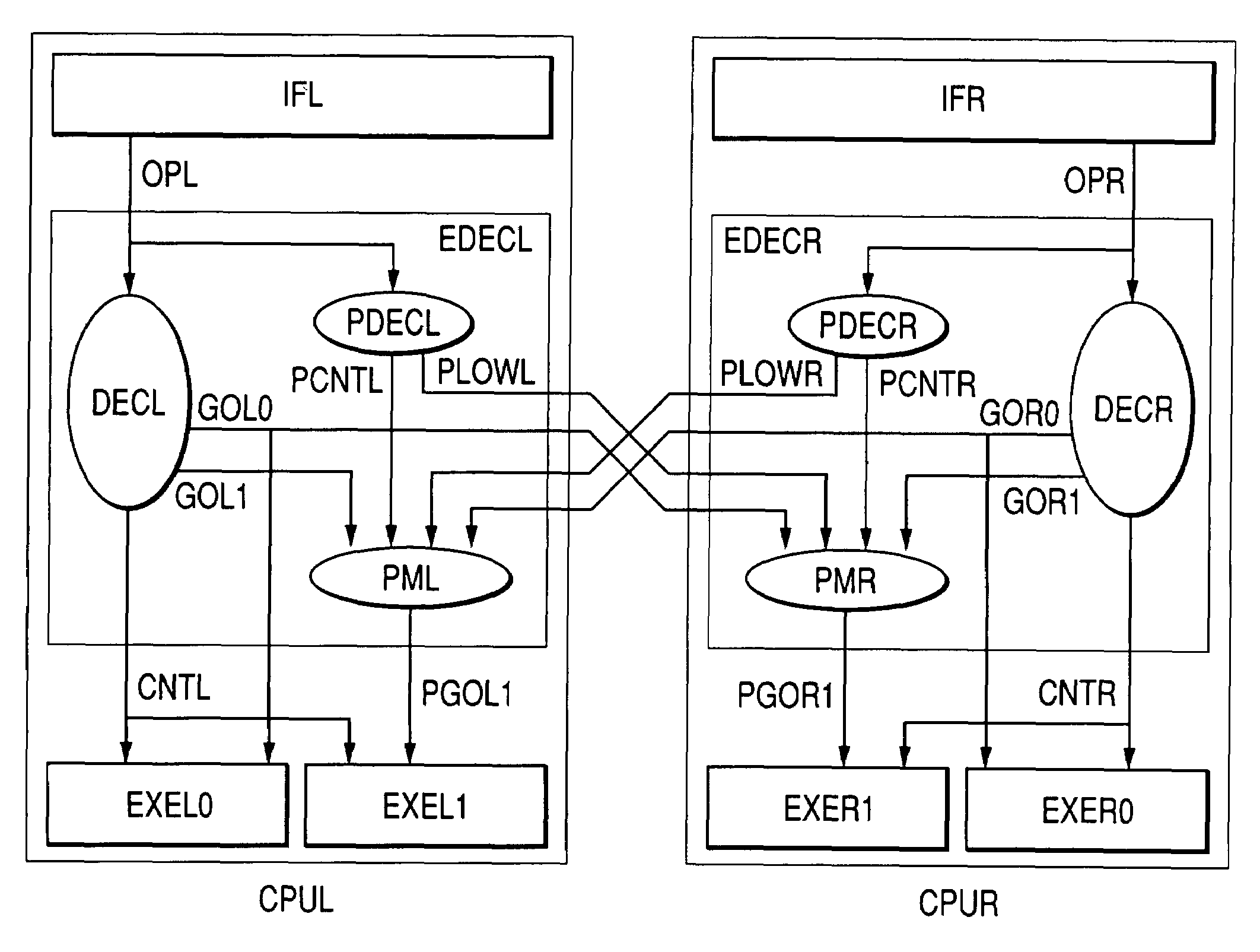
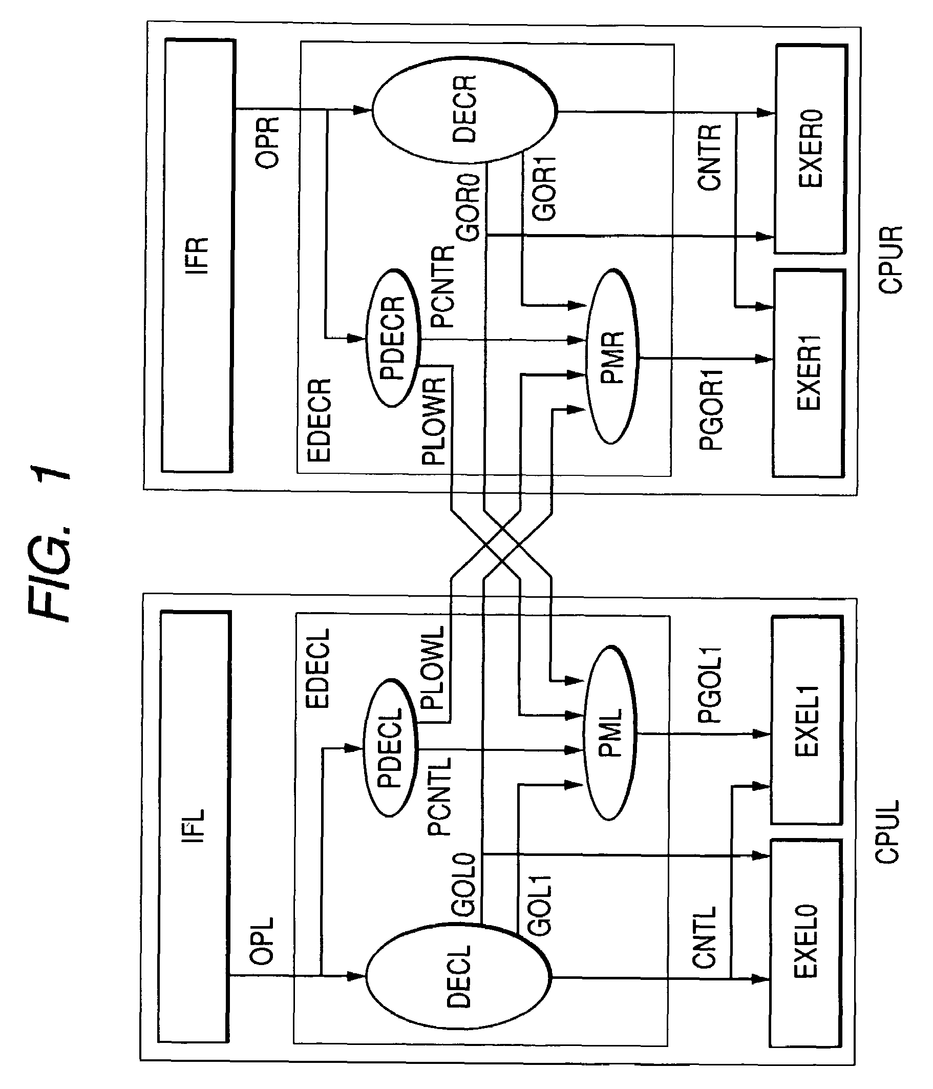
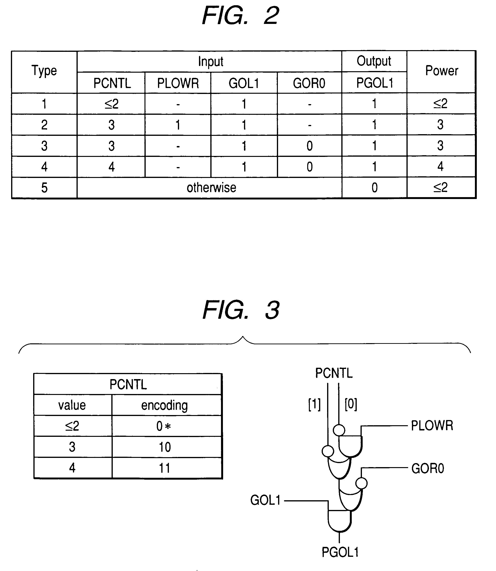
[0057]A first embodiment of the present invention will be described below with reference to FIGS. 1 to 3. FIG. 1 shows the configuration of a semiconductor device according to the first embodiment of the present invention. FIG. 2 shows a control truth value table for a power control section according to the first embodiment. FIG. 3 shows a control logic for the power control section of the first embodiment.

[0058]In the present embodiment, two processors CPUL and CPUR, each having an equal maximum power consumption, notifies each other of expected power consumption and each processor controls power consumption thereof so that the total sum of power consumptions for each cycle is equal to or less than allowable power. One cycle, as used in the present embodiment, corresponds to one instruction.

[0059]In the present embodiment, allowable power for the two processors equals half of the total sum of the maximum power consumptions and each processor keeps operating on half of the maximum p...

second embodiment

[0078]A second embodiment of the present invention will be described below with reference to FIGS. 4 to 6. FIG. 4 shows the configuration of a semiconductor device according to the second embodiment of the present invention. FIG. 5 shows a control truth value table for a power control section according to the second embodiment. FIG. 6 shows a control logic for the power control section of the second embodiment.

[0079]In the present embodiment, two processors CPUL and CPUR, each having a equal maximum power consumption, notify each other of expected power consumption and each processor controls power consumption thereof so that the total sum of power consumptions during two cycles for the two processors is equal to or less than allowable power. Further, as with the first embodiment, one cycle, as used in the present embodiment, corresponds to one instruction.

[0080]Allowable power for the two processors equals half of the total sum of the maximum power consumptions during two cycles. E...

third embodiment

[0102]A third embodiment of the present invention will be described below with reference to FIGS. 7 to 9. FIG. 7 shows the configuration of a semiconductor device according to the third embodiment of the present invention. FIG. 8 shows a control truth value table for a power control section according to the third embodiment. FIG. 9 shows a control logic for the power control section of the third embodiment.

[0103]In the present embodiment is, as with the first embodiment, two processors CPUL and CPUR, each having an equal maximum power consumption, notifies each other of expected power consumption and each processor controls power consumption thereof so that the total sum of power consumptions during each cycle may be equal to or less than allowable power. In the present embodiment, each processor is a scholar processor that executes instructions one by one. The maximum power consumption at which the processor issues one instruction is 2. The allowable power for the two processors is...


PUM


Abstract

The disclosure describes a semiconductor device having a plurality of modules each enabled to perform properly while managing allowable power for an entire chip through distributed power control. A predetermined allowable power consumption value is defined for each module. The predetermined power consumption value refers to power consumption defined taking into account allowable power values for a plurality of modules. Each module takes a difference between the predetermined allowable power consumption value and an actual power consumption value as extra power and notifies other modules of the extra power thereof. To avoid a deadlock, each module is designed to be capable of performing data processing below the predetermined power consumption value without using extra power from another module. When notified of extra power by another module, each module can use for data processing power equal to the predetermined power consumption thereof and the extra power.

Description

CLAIMS OF PRIORITY [0001]The present application claims prority from Japanese application JP 2004-154232 filed on May 25, 2004, the content of which is hereby incorporated by reference into this application.BACKGROUND OF THE INVENTION [0002]The prevent invention relates to data processing devices and semiconductor devices. More specifically, the present invention relates preferably to a semiconductor device in which a plurality of processors are composed of integrated circuits, in particular, CMOS circuits which change in power consumption depending on the operational states thereof, and which semiconductor device allows the processors to exhibit those performance well while minimizing the power consumption for the entire semiconductor chip.[0003]With the expansion of portable device markets including a cellular phone market, there is growing importance of semiconductor chips operable even at a low power. It is desirable that the maximum power consumption, the average power consumpt...

Claims


Application Information

Patent Timeline
Patent Type & Authority Patents(United States)
IPC IPC(8): G06F1/32G06F1/28G06F1/30G06F15/78H01L21/822H01L27/04
CPCG06F1/3203G06F1/3287G06F9/3869G06F9/3836Y02B60/1282Y02D10/00
Inventor ARAKAWA, FUMIO
Owner HITACHI LTD
Learn More