Semiconductor device and method of manufacturing the same

a semiconductor and semiconductor technology, applied in the field of semiconductor devices, can solve the problems of easy cracking and heavy, glass substrates and quartz substrates are difficult to be made larger, and cannot help lowering the highest temperature of the process

Inactive Publication Date: 2008-02-19
SEMICON ENERGY LAB CO LTD
View PDF98 Cites 187 Cited by
  • Summary
  • Abstract
  • Description
  • Claims
  • Application Information

AI Technical Summary

Benefits of technology

[0014]The thickness of the bonding member can be set appropriately. If the bonding member is thinner than the plastic film, the semiconductor device can be thinner, more light-weight, and more flexible. When the bonding member alone holds the layer including the element, the total thickness can be 0.5 mm or less, preferably 0.1 mm to 0.3 mm or less, for example.
[0050]In the above structure, the manufacture method is characterized in that the protective film is a silicon nitride film or a silicon oxynitride film. By forming the protective film, moisture and impurities from the outside can be effectively blocked to avoid contamination.

Problems solved by technology

At present, although many glass substrates and quartz substrates are utilized, there are defaults of being easily cracked and heavy.
Moreover, the glass substrates and quartz substrates are difficult to be made larger in terms of conducting a mass-production, and these are not suitable for that.
However, since the heat resistance of a plastic film is low, it cannot help lowering the highest temperature of the process.
As a result, at present, a TFT is formed which has not so excellent electric characteristics compared with those formed on the glass substrates.
Therefore, a liquid crystal display device and light emitting element having a high performance by utilizing a plastic film have not been realized yet.
Moreover, since the transparency of plastic film to the light is lower than that of glass substrate, it is not based on the quality of the material and thickness of a plastic film which pass light, but there is also a problem that the transparency become worse slightly.

Method used


Image

  • Semiconductor device and method of manufacturing the same
  • Semiconductor device and method of manufacturing the same
  • Semiconductor device and method of manufacturing the same

Examples


embodiment mode 1

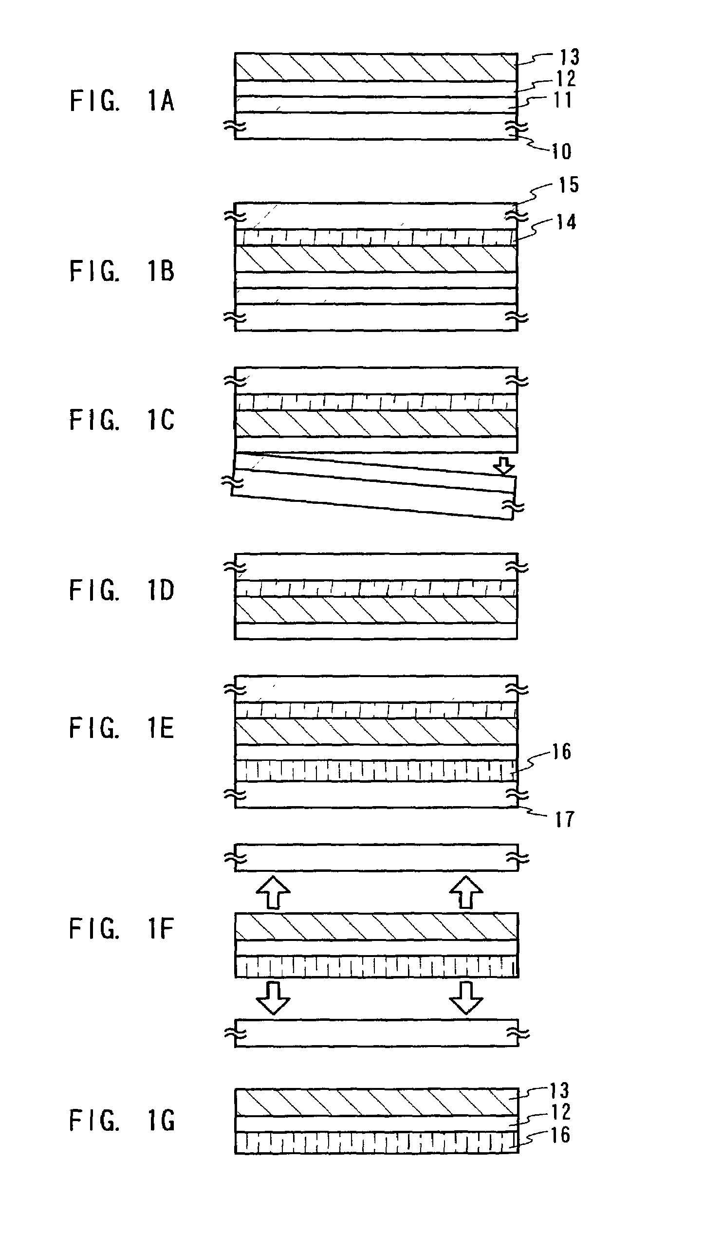
[0072]The following is a brief description on a typical peeling procedure and semiconductor device manufacturing method using the present invention. The description will be given with reference to FIGS. 1A to 1G.

[0073]In FIG. 1A, reference numeral 10 denotes a first substrate, 11, a first material layer that is a nitride layer or a metal layer, 12, a second material layer that is an oxide layer, and 13, a layer to be peeled.

[0074]The first substrate 10 in FIG. 1A can be a glass substrate, a quartz substrate, a ceramic substrate, or the like. A semiconductor substrate, typically a silicon substrate, or a metal substrate, typically a stainless steel substrate, may also be used.

[0075]First, the first material layer 11 is formed on the substrate 10 as shown in FIG. 1A. The first material layer 11 may have compressive stress or tensile stress immediately after it is formed. However, it is important to use for the first material layer 11 a material which is free from peeling or other dist...

embodiment mode 2

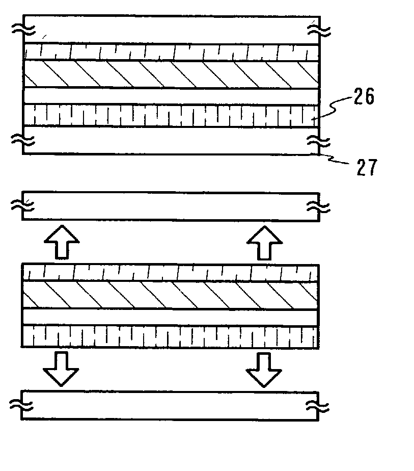
[0096]Embodiment Mode 1 shows an example in which the second bonding member alone serves as a supporter. In this embodiment mode, an example of using the first bonding member and the second bonding member as a supporter is shown. FIGS. 2A to FIGS. 2E are roughly identical with FIGS. 1A to 1E. Therefore, detailed descriptions will be omitted here and only differences between Embodiment Mode 1 and Embodiment Mode 2 will be described.

[0097]In FIGS. 2A to 2G, reference numeral 20 denotes a first substrate, 21, a first material layer that is a nitride layer or a metal layer, 22, a second material layer that is an oxide layer, 23, a layer to be peeled, 24, a first bonding member, 25, a second substrate, 26, a second bonding member, and 27, a third substrate.

[0098]First, according to Embodiment Mode 1, there is obtained a state of FIG. 2E in the same procedure.

[0099]Here, reaction-cured adhesives, thermally-curable adhesives, photo-curable adhesives such as UV-curable adhesives, anaerobic ...

embodiment mode 3

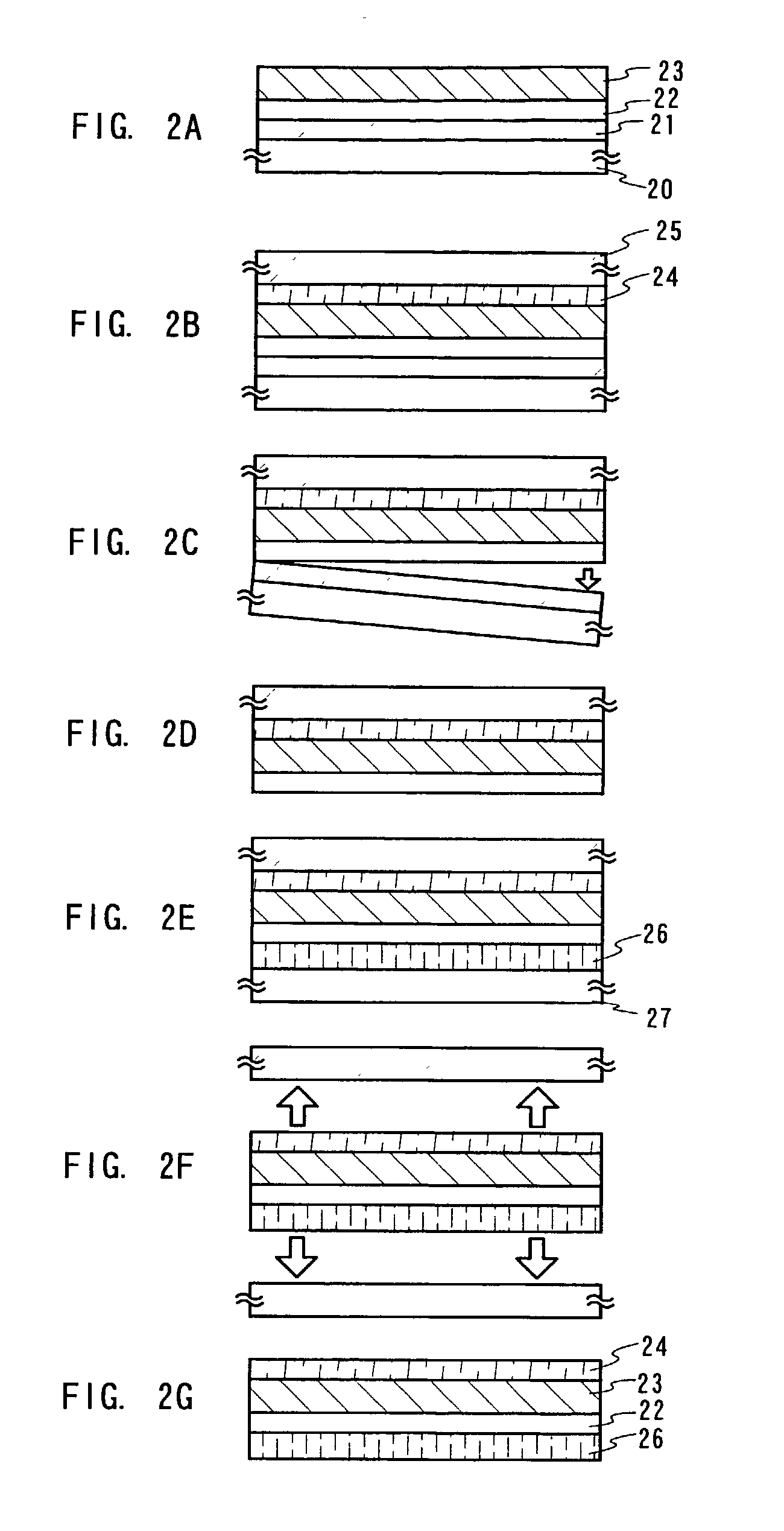
[0109]Embodiment Mode 1 shows an example in which the second bonding member alone serves as a supporter. In this embodiment mode, an example of using the second bonding member and the third substrate as a supporter is shown. FIGS. 3A to 3E are roughly identical with FIGS. 1A to 1E. Therefore detailed descriptions will be omitted here and only differences between Embodiment Mode 1 and Embodiment Mode 2 will be described.

[0110]In FIGS. 3A to 3G, reference numeral 30 denotes a first substrate, 31, a first material layer that is a nitride layer or a metal layer, 32, a second material layer that is an oxide layer, 33, a layer to be peeled, 34, a first bonding member, 35, a second substrate, 36, a second bonding member, and 37, a third substrate.

[0111]First, according to Embodiment Mode 1, there is obtained a state of FIG. 3E in the same procedure.

[0112]The first substrate 30 can be a glass substrate, a quartz substrate, a ceramic substrate, or the like. A semiconductor substrate, typical...


PUM

PropertyMeasurementUnit
total thicknessaaaaaaaaaa
temperatureaaaaaaaaaa

Abstract

A semiconductor device having a semiconductor element (a thin film transistor, a thin film diode, a photoelectric conversion element of silicon PIN junction, or a silicon resistor element) which is light-weight, flexible (bendable), and thin as a whole is provided as well as a method of manufacturing the semiconductor device. In the present invention, the element is not formed on a plastic film. Instead, a flat board such as a substrate is used as a form, the space between the substrate (third substrate (17)) and a layer including the element (peeled layer (13)) is filled with coagulant (typically an adhesive) that serves as a second bonding member (16), and the substrate used as a form (third substrate (17)) is peeled off after the adhesive is coagulated to hold the layer including the element (peeled layer (13)) by the coagulated adhesive (second bonding member (16)) alone. In this way, the present invention achieves thinning of the film and reduction in weight.

Description

BACKGROUND OF THE INVENTION[0001]1. Field of the Invention[0002]The present invention relates to a semiconductor device having a circuit consisted of a thin film transistor (hereinafter, referred to as TFT) and a method of manufacturing the semiconductor device. For example, the present invention relates to an electro-optic device that is represented by a liquid crystal module, a light emitting device that is represented by an electroluminescence display device and an electronic device on which such a device is mounted as a part.[0003]It should be noted that in the present specification, the term “semiconductor device” indicates a device in general capable of functioning by utilizing the semiconductor characteristics, and an electro-optic device, a light emitting device, a semiconductor circuit and an electronic equipment are all semiconductor devices.[0004]2. Related Art[0005]In recent years, a technology constituting a thin film transistor (TFT) using a semiconductor thin film (in...

Claims


Application Information

Patent Timeline
Patent Type & Authority Patents(United States)
IPC IPC(8): H01L21/00G02F1/1368H01L21/02H01L21/336H01L21/77H01L21/84H01L27/12H01L27/32H01L29/786H01L51/50H01L51/56H05B33/02H05B33/14
CPCH01L27/1214H01L27/1266H01L51/56H01L29/78603H01L51/0024H01L27/32H01L27/1218H10K59/00H10K71/50H10K71/00H01L27/12H01L21/308H01L21/76251H01L21/76275
Inventor MARUYAMA, JUNYATAKAYAMA, TORUGOTO, YUUGO
Owner SEMICON ENERGY LAB CO LTD
Why Eureka
Try Eureka