Method of fabricating crossing wiring pattern on a printed circuit board

a printed circuit board and cross-wiring technology, applied in the direction of transportation and packaging, non-printed electrical components of printed circuits, metal adhesion improvement of insulating substrates, etc., can solve the problems of exponentially complex manufacturing process, short-circuit wiring, etc., and achieve the effect of improving resolution

Inactive Publication Date: 2008-02-19
IBIDEN CO LTD
View PDF45 Cites 18 Cited by
  • Summary
  • Abstract
  • Description
  • Claims
  • Application Information

AI Technical Summary

Benefits of technology

[0031]In the printed wiring board of claim 3, the fillet is added to the crossing portion of the wiring pattern of the printed wiring board and no stress is concentrated to the crossing portion so that no wiring pattern is disconnected. Further, no air bubbles are left between the crossing portion of the wiring pattern and the interlayer resin insulating layer so that reliability of the printed wiring board is improved.
[0041]A mixing ratio of the thermosetting resin (photosensitive resin) and the thermoplastic resin is preferably set such that thermosetting resin (photosensitive resin) / thermoplastic resin=95 / 5 to 50 / 50. This is because a high toughness value can be secured without reducing a heating resisting property.
[0046]There is a case in which such a solder resist layer is separated since the solder resist layer is constructed by resin having a stiff skeleton. Therefore, the separation of the solder resist layer can be also prevented by arranging a reinforcing layer.
[0052]In the solder resist layer using such a composition substance, no free acid is caused and no copper pad surface is oxidized. Further, a harmful property with respect to a human body is low.
[0055]As explained above, various kinds of antifoaming and leveling agents, thermosetting resin for improving a heat resisting property and an antibasic property and giving a flexible property, a photosensitive monomer for improving resolution, etc. can be further added to the solder resist composition substance.
[0059]A polyhydric acrylic-system monomer can be used as the above photosensitive monomer as an adding component since the polyhydric acrylic-system monomer can improve resolution. For example, DPE-6A manufactured by NIHON KAYAKU and R-604 manufactured by KYOEISYA KAGAKU can be used as the polyhydric acrylic-system monomer.

Problems solved by technology

However, when these values are set smaller than the above minimum values respectively, no desirable wiring can be formed by dispersion of a slight process condition in order that the probability of generation of disconnection of the wiring, a short-circuit of wirings, etc. is increased and yield is reduced.
However, if the number of build-up layers is increased, a manufacturing process becomes exponentially complicated and reliability and yield are reduced.
Therefore, it is difficult to improve performance of the multilayer build-up wiring board.
However, in this light etching, no etching liquid can be sufficiently moved around the high wiring density portion so that the thickness of the wiring pattern can be increased.
However, in a land shape of the prior art, a through hole distance is widened to hold mutual insulation of the inner layer pad and the number of through holes formed in the multilayer core substrate is limited by this land shape.
However, as mentioned above, the number of through holes able to be formed in the multilayer core substrate is limited.
However, when the number of build-up wiring layers on the front and rear sides are set to be different to each other, a warp is caused by an asymmetric property.
Namely, in the printed wiring board (package substrate) of the prior art, since the number of build-up layers is increased, problems exist whereby the connection reliability of upper and lower layers is reduced and the cost of the package substrate is increased and, thickness and weight of the package substrate is excessively increased.

Method used


Image

  • Method of fabricating crossing wiring pattern on a printed circuit board
  • Method of fabricating crossing wiring pattern on a printed circuit board
  • Method of fabricating crossing wiring pattern on a printed circuit board

Examples


first embodiment

[0095]Here, the explanation is made with respect to compositions of A. an adhesive for electroless plating, B. an interlayer resin insulating agent, and C. a resin filling agent used in the manufacturing method of the multilayer printed wiring board in accordance with the

A. Raw Material Composition Substance for Adjusting and Manufacturing an Adhesive for Electroless Plating (an Adhesive for an Upper Layer)

[0096][Resin Composition Substance ①]

[0097]A resin composition substance is obtained by stirring and mixing 35 weight parts of a resin liquid, 3.15 weight parts of a photosensitive monomer (manufactured by TO-A GOSEI, Alonix M315), 0.5 weight part of an antifoaming agent (manufactured by SAN-NOPUKO, S-65) and 3.6 weight parts of NMP. In the resin liquid, 25% of a cresol novolak type epoxy resin (manufactured by NIHON KAYAKU, molecular weight 2500) and 80 wt % of an acrylic substance in concentration are dissolved to DMDG.

[0098][Resin Composition Substance ②]

[0099]A resin compositi...

second embodiment

[0167]A multilayer build-up wiring board in accordance with the present invention will next be explained with reference to the drawings.

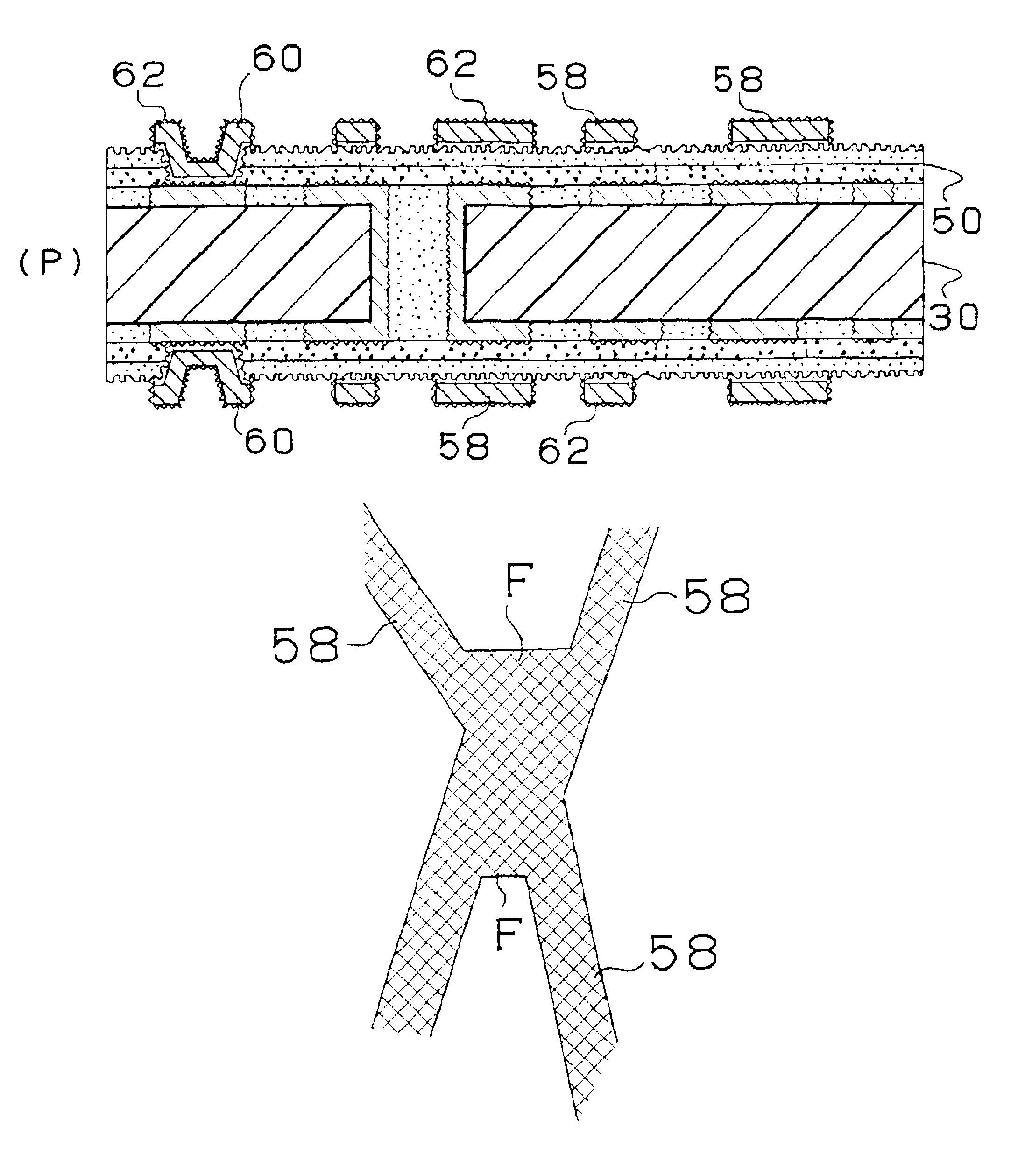
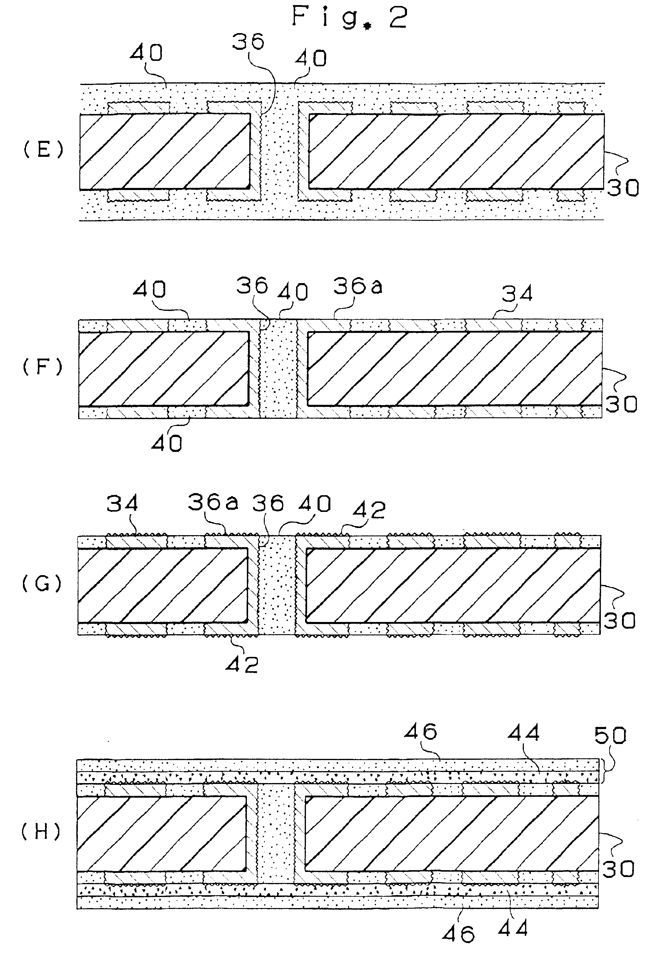
[0168]FIG. 13 shows a section of the multilayer build-up wiring board in accordance with the second embodiment of the present invention. Build-up wiring layers 90A, 90B are formed on front and rear faces of a multilayer core substrate 30. The build-up layers 90A, 90B are constructed by interlayer resin insulating layers 50 and 150. A via hole 60, a via hole land 61 and a wiring pattern 58 are formed in the interlayer resin insulating layer 50. A via hole 160, a land 161 and an unillustrated wiring pattern are formed in the interlayer resin insulating layer 150. The via hole 160 in an upper layer is connected to the via hole land 61.

[0169]A soldering bump 76U for connection to an unillustrated bump of an IC chip is formed on a front (upper face) side of the printed wiring board. A soldering bump 76D for connection to an unillustrated bump of a mother...

third embodiment

[0179]A printed wiring board and its manufacturing method in accordance with the present invention will next be explained with reference to the drawings.

[0180]First, the construction of the printed wiring board 10 in accordance with the third embodiment of the present invention will be explained with reference to FIGS. 17 and 18. FIG. 17 shows a state in which an IC chip 90 is mounted to the multilayer printed wiring board 10 and is attached to a daughter board 94.

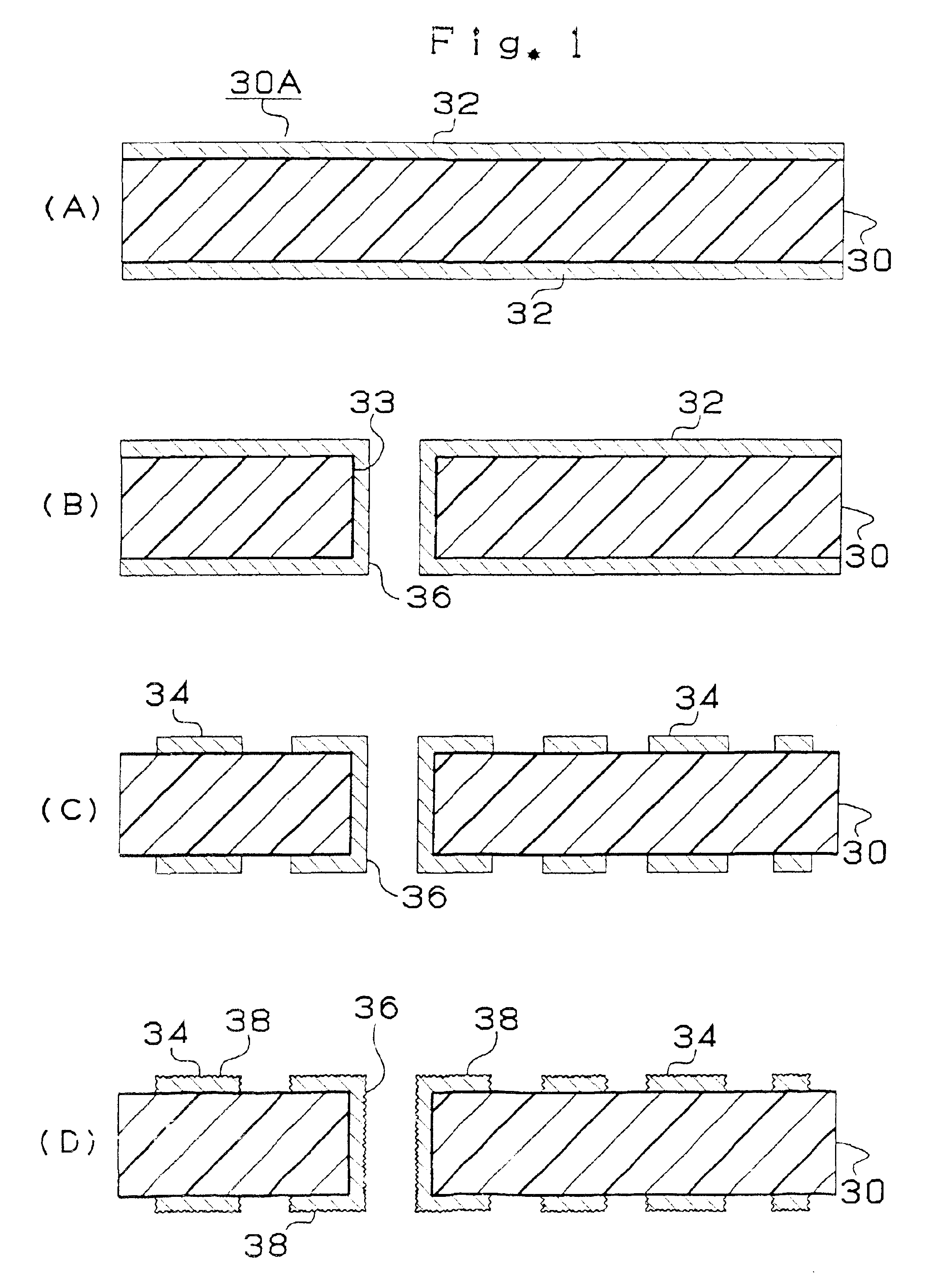
[0181]As shown in FIG. 17, a through hole 36 is formed within a core substrate 30 in the printed wiring board 10, and a conductor circuit 34 is formed on each of both faces of the core substrate 30. A lower layer side interlayer resin insulating layer 50 is formed on the core substrate 30. A conductor layer constructed by a via hole 60, a wiring pattern 58S, a land 58R and a dummy conductor 58D is formed in the lower layer side interlayer resin insulating layer 50. An upper layer interlayer resin insulating layer 150 is ar...


PUM

PropertyMeasurementUnit
angleaaaaaaaaaa
anglesaaaaaaaaaa
widthaaaaaaaaaa

Abstract

A filet F is added to a portion constituting a corner portion C equal to or smaller than 90° in a crossing portion X of wiring patterns 58b, 58c and 58d, and a wiring pattern 58 is formed. Since the filet F is added, the wiring patterns are not made thin and are not disconnected in the crossing portion X. Further, since there is no stress concentrated to the crossing portion X, disconnection is not caused in the wiring patterns and no air bubbles are left between the crossing portion X of the wiring patterns and an interlayer resin insulating layer so that reliability of a printed wiring board is improved.

Description

[0001]This is a Continuation of National Application No. 09 / 700,592 filed Nov. 17, 2000, now U.S. Pat. No. 6,407,345 which is a 371 of PCT / JP99 / 02512, filed May 13, 1999.TECHNICAL FIELD[0002]This invention relates to a printed wiring board forming a wiring pattern thereon and in particular relates to a printed wiring board able to be suitably used in a multilayer build-up wiring board and a manufacturing method of the printed wiring board.BACKGROUND ART[0003]A method for alternately building-up an insulating layer and a conductor layer in a core substrate is adopted at present to realize an increase in density of the multilayer printed wiring board. Here, there are two kinds of methods constructed by full additive and semi-additive methods as the built-up method. A manufacturing process of a conductor circuit onto an interlayer resin insulating layer of the multilayer printed wiring board using this semi-additive method will be explained next with reference to FIG. 32.[0004]First, a...

Claims


Application Information

Patent Timeline
Patent Type & Authority Patents(United States)
IPC IPC(8): H01L23/48H05K1/11H01K7/00H05K1/02H05K3/18H05K3/24H05K3/38H05K3/46
CPCH05K1/0256H05K1/0271H05K1/113H05K1/115H05K3/4602Y10T29/49155H05K1/0265H05K1/116H05K3/184H05K3/241H05K3/382H05K3/4661H05K2201/09227H05K2201/09236H05K2201/09254H05K2201/09272H05K2201/09454H05K2201/09536H05K2201/0959H05K2201/09627H05K2201/09727H05K2201/09781H05K2201/10734H05K2203/0594H01L2224/16225Y10T29/49194H05K1/0263H01L2224/05573H01L2224/05568Y10T428/31504H01R12/00H05K3/46H01L23/48H01L23/12
Inventor HIROSE, NAOHIROKARIYA, TAKASHIMORI, YOJI
Owner IBIDEN CO LTD
Why Eureka
Try Eureka