Static random access memory device having reduced leakage current during active mode and a method of operating thereof

a random access memory and static technology, applied in static storage, information storage, digital storage, etc., can solve the problems of undesirable operating problems of the smaller sram device, increased current leakage, and reduced leakage current, so as to achieve enhanced low operating voltage vess

Active Publication Date: 2008-02-19
TEXAS INSTR INC
View PDF13 Cites 17 Cited by
  • Summary
  • Abstract
  • Description
  • Claims
  • Application Information

AI Technical Summary

Benefits of technology

[0011]The present invention, therefore, may provide a greater power savings and a better SNM and write trip voltage Vtrip trade-off than existing SRAM devices allowing a wider process margin. Providing the enhanced low operating voltage VESS reduces current leakage IDDQ by lowering voltage across the memory cell and raising the threshold voltage Vtn due to a back bias effect since the enhanced low operating voltage VESS is greater than a substrate voltage (typically the low operating voltage VSS). The SNM may be improved by the higher Vtn from the back bias effect that adequately compensates for the lowering of the SNM by a reduced cell voltage. With an improved SNM, cells may suffer a minimum of upset when the associated word line voltage is raised for access, as in a READ, or for non-addressed columns in an accessed row for WRITE. Similarly, the improved SNM may allow WRITE operations without upsetting cells in unaddressed columns.
[0014]In another aspect, the present invention provides a method of operating an SRAM device including (1) employing in an integrated circuit an SRAM array coupled to row peripheral circuitry by a word line and coupled to column peripheral circuitry by bit lines and (2) providing an enhanced low operating voltage VESS to the SRAM array during at least a portion of an active mode.

Problems solved by technology

Desired miniaturization, however, may include undesirable operating problems for the smaller SRAM devices.
For example, current leakage may increase as the size of SRAM devices decreases.
Current leakage may provide a problem during a sleep mode, a standby mode and even during an active mode.
This alternative, unfortunately, requires more switching power and does not support the write trip voltage Vtrip.
If SNM is too low, READ operations may be disrupted.
If Vtrip is too low, WRITE operations may be disrupted.
Unfortunately, the requirements for an acceptable SNM and write trip voltage Vtrip may limit the tolerances for an acceptable SRAM yield during manufacturing since increasing one typically decreases the other.
For example, a strong n-channel can cause SNM to be unsuitably low, particularly when accompanied by a weak p-channel.
However, a weak n-channel can cause Vtrip to be unsuitably low, particularly when accompanied by a strong p-channel.
Thus, existing SRAM devices are challenged by the competing and contradicting objectives of providing a weak n-channel (and / or a strong p-channel) to achieve an acceptable SNM and providing a strong n-channel (and / or a weak p-channel) to achieve an acceptable Vtrip.

Method used


Image

  • Static random access memory device having reduced leakage current during active mode and a method of operating thereof
  • Static random access memory device having reduced leakage current during active mode and a method of operating thereof
  • Static random access memory device having reduced leakage current during active mode and a method of operating thereof

Examples


Embodiment Construction

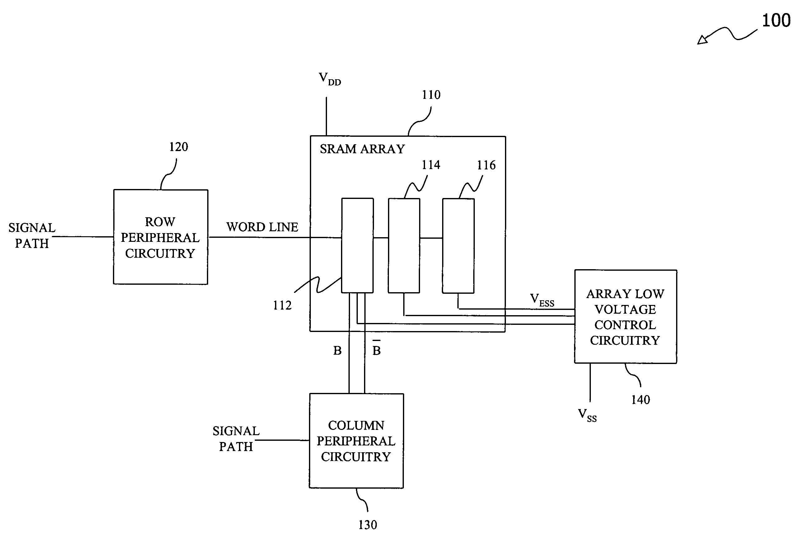
[0019]Referring initially to FIG. 1, illustrated is a circuit diagram of an embodiment of an SRAM device, generally designated 100, constructed according to the principles of the present invention. The SRAM device 100 includes an SRAM array 110, row peripheral circuitry 120, column peripheral circuitry 130 and an array low voltage control circuitry 140. Typically, the SRAM array 110 includes multiple memory cells organized in a matrix of columns and rows with corresponding multiple word lines and bit lines. For example, the SRAM array 110 may have 256 columns and 256 rows of memory cells. For ease of discussion, however, only a single row with a first, second and third column 112, 114, 116, of the SRAM array 110 are illustrated. Furthermore, only a single word line, bit line pair, row peripheral circuitry 120 and column peripheral circuitry 130 associated with the first column 112 are illustrated and discussed. One skilled in the art, however, will understand that the illustrated an...


PUM


Abstract

An Static Random Access Memory (SRAM) device and a method of operating the same. In one embodiment, the SRAM device includes: (1) an SRAM array coupled to row peripheral circuitry by a word line and coupled to column peripheral circuitry by bit lines and (2) an array low voltage control circuitry that provides an enhanced low operating voltage VESS to the SRAM array during at least a portion of an active mode thereof.

Description

TECHNICAL FIELD OF THE INVENTION[0001]The present invention is directed, in general, to memory devices and, more specifically, to a Static Random Access Memory (SRAM) device having reduced leakage current during active mode and a method of operating thereof.BACKGROUND OF THE INVENTION[0002]Memory devices are well known in the art and used in, among other things, virtually all microprocessor and digital signal processor (DSP) applications. One type of memory favored for many applications is Static Random Access Memory (SRAM). SRAM devices are fast and easy to use relative to many other types of memory devices. In addition, SRAM devices using metal-oxide-semiconductor (MOS) technology exhibit relatively low standby power and do not require a refresh cycle to maintain stored information. These attributes make SRAM devices particularly desirable for battery-powered equipment, such as laptop computers and personal digital assistants.[0003]Miniaturization of SRAM devices is another attrib...

Claims


Application Information

Patent Timeline
Patent Type & Authority Patents(United States)
IPC IPC(8): G11C11/00G11C11/417
CPCG11C11/417
Inventor HOUSTON, THEODORE W.
Owner TEXAS INSTR INC
Why Eureka
Try Eureka