Method and system for device level simulation of large semiconductor memories and other circuits

a semiconductor memory and circuit technology, applied in the field of device level simulation of large semiconductor memory and other circuits, can solve the problems of long-standing challenges, inability to effectively simulate or verify large semiconductor memory circuits, and impracticality of use for this purpos

Active Publication Date: 2008-02-19
NAT SEMICON CORP
View PDF8 Cites 6 Cited by
  • Summary
  • Abstract
  • Description
  • Claims
  • Application Information

AI Technical Summary

Problems solved by technology

Simulation and verification of large semiconductor memory netlists (and other large netlists) whose elements model MOS transistors, voltage sources, resistors, and capacitors has long been a very challenging task.
Conventional simulators (e.g., conventional SPICE based simulators) cannot be used effectively to simulate or verify large semiconductor memory circuits since the circuits are usually too large for such simulators to handle.
Even conventional simulators which can handle large netlists typically require too much time to simulate and verify a design for a large semiconductor memory circuit, by reading and writing every memory address, and thus are typically impractical to use for this purpose.
Also, typical conventional simulators (e.g., SPICE based simulators) cannot detect unknown (“X”) states or high impedance states at nets in electrical circuits of any type.
Furthermore, the high degree of accuracy offered by commonly used conventional simulators is typically unnecessary for verification of large semiconductor memory circuits since only functional verification, and not accurate timing and power calculation, is typically required for large semiconductor memory circuit verification.
Typically also, event driven digital simulators (e.g., those

Method used


Image

  • Method and system for device level simulation of large semiconductor memories and other circuits
  • Method and system for device level simulation of large semiconductor memories and other circuits
  • Method and system for device level simulation of large semiconductor memories and other circuits

Examples


Embodiment Construction

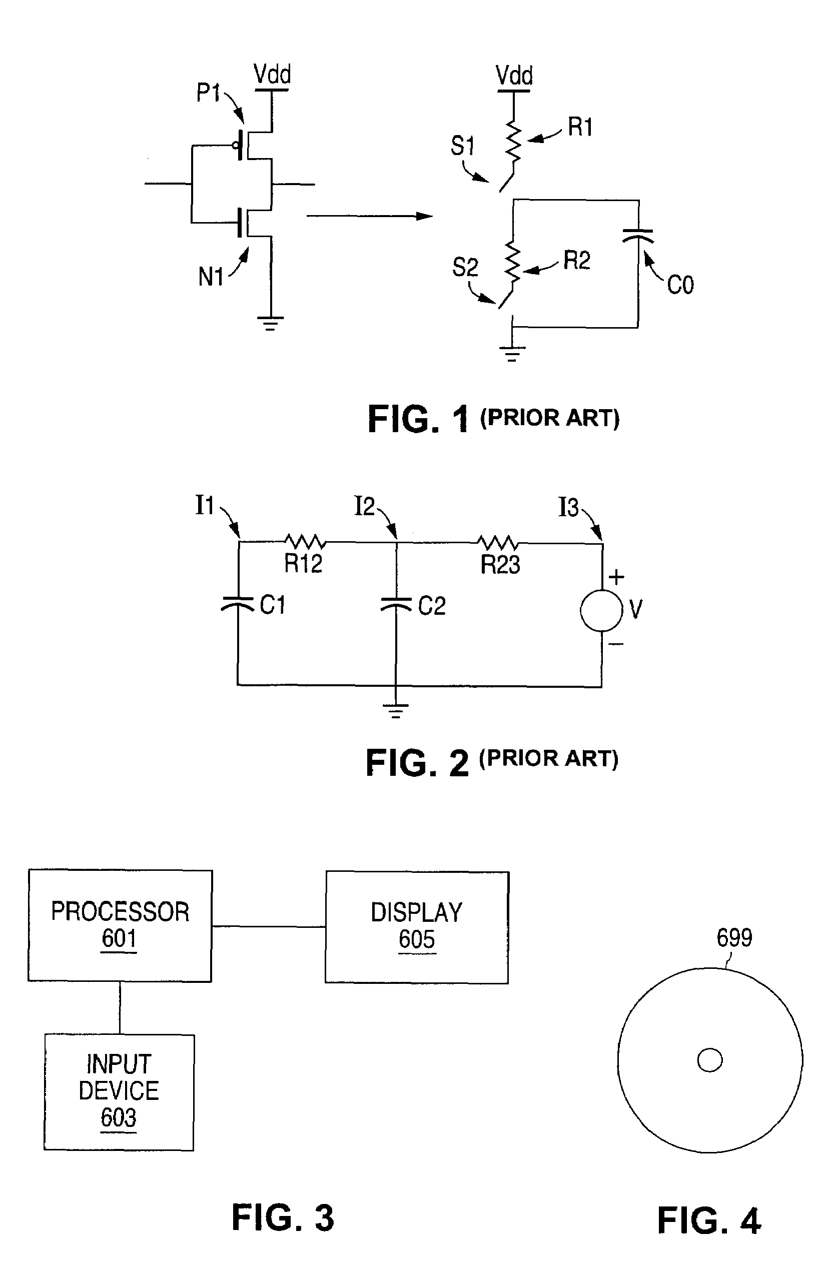
[0012]In a class of embodiments, the invention is a method for device level simulation of a circuit modeled by a set of CCR graphs, wherein the circuit includes MOS transistors having unknown gate potentials, each of the CCR graphs includes a top rail, and a bottom rail, and variable nodes (i.e., some number, “N,” of variable nodes), each of the transistors having unknown gate potential is modeled in the CCR graphs as a selectable resistor and optionally also at least one other element (e.g., a capacitor), and each said selectable resistor has a selected one of a first resistance and a second resistance much larger than the first resistance. The method includes the steps of: (a) determining potentials Von1, Von2, . . . , VonN, at the variable nodes (of one of the CCR graphs) with each selectable resistor of the graph having its first resistance and without determining effective resistances between the variable nodes and the top rail or the bottom rail, where Voni is the potential at...


PUM


Abstract

A method for device level simulation of a circuit modeled by a set of CCR graphs, a computer system programmed to perform such a method, and a computer readable medium which stores code for implementing such a method. Typically, the circuit includes MOS transistors having unknown gate potentials, each CCR graph includes a top rail, and a bottom rail, and variable nodes, each of the transistors having unknown gate potential is modeled in the CCR graphs as a selectable resistor having a selected one of a first resistance and a much larger second resistance, and the method includes the steps of determining potentials at variable nodes of one of the CCR graphs with each selectable resistor of the graph having its first resistance (and also with each selectable resistor of the graph having its second resistance) without determining effective resistances between the variable nodes of the graph and the top rail or bottom rail.

Description

BACKGROUND OF THE INVENTION[0001]1. Field of the Invention[0002]The present invention pertains to methods and systems (e.g., programmed computer systems) for device level simulation of semiconductor memory circuits and other circuits comprising MOS transistors.[0003]2. Description of the Related Art[0004]The term “netlist” will be used herein to denote a description of the connectivity of a circuit comprising elements. A netlist consists of predefined elements (e.g., resistors, capacitors, and switches) connected together by “nets.” Each net is a conductor, and will sometimes be referred to herein as a node. The term “graph” will sometimes be used herein to denote a netlist.[0005]Simulation and verification of large semiconductor memory netlists (and other large netlists) whose elements model MOS transistors, voltage sources, resistors, and capacitors has long been a very challenging task. Conventional simulators (e.g., conventional SPICE based simulators) cannot be used effectively...

Claims


Application Information

Patent Timeline
IPC IPC(8): G06F17/00
CPCG06F17/5036G06F30/367
Inventor DASTIDAR, TATHAGATO RAIRAY, PARTHA
Owner NAT SEMICON CORP
Why Eureka
Try Eureka