Method for manufacturing a light-emitting diode

a technology of light-emitting diodes and manufacturing methods, which is applied in the direction of electrical apparatus, nanotechnology, semiconductor devices, etc., can solve the problems of reducing productivity, short circuit in the device, and greatly increasing costs, so as to improve yield and throughput, reduce manufacturing costs, and improve manufacturing efficiency

Inactive Publication Date: 2008-02-26
EPISTAR CORP
View PDF13 Cites 51 Cited by
  • Summary
  • Abstract
  • Description
  • Claims
  • Application Information

AI Technical Summary

Benefits of technology

[0009]In accordance with the disadvantages caused by the conventional process for manufacturing a light-emitting diode, one objective of the present invention is to provide a method for manufacturing a light-emitting diode, in which an insulating etching mask layer is formed on a transparent conductive oxide layer, so that the contamination resulting from the use of metal mask materials can be avoided, to prevent the short circuit condition caused by the metal mask materials from occurring.
[0010]Another objective of the present invention is to provide a method for manufacturing a light-emitting diode, in which a transparent conductive oxide layer and epitaxial layers are etched by a self-aligned method, so that there is no mask employed in the etching processes of the transparent conductive oxide layer and the epitaxial layers. Accordingly, the amount of the masks is decreased, and the illuminative area of the device is increased to enhance the brightness of the device.
[0011]Still another objective of the present invention is to provide a method for manufacturing a light-emitting diode, in which only two masks are employed in the manufacturing process, so that the process cost is lowered, the amount of the process steps is decreased, the process time is shortened, and the throughput and the yield are effectively enhanced.
[0014]By deposing a dielectric mask layer on a transparent conductive oxide layer, the fabrication of a light-emitting diode structure is completed while only two masks are employed, and the transparent conductive oxide layer and epitaxial layers can be etched by a self-aligned method. Accordingly, the manufacture cost is lowered and the illuminative area is increased to achieve the purposes of enhancing the brightness, the yield and the throughput.

Problems solved by technology

In the processing of the conventional light-emitting diode, because the nickel metal layer 110 is used as the etching mask, the contamination of metal material may occur to result in a short circuit in the device.
Moreover, in the entire process, five masks are needed, so that the cost is greatly increased, many extra process steps are added, the process time is prolonged to result in lowered productivity, and the product yield is adversely affected.

Method used


Image

  • Method for manufacturing a light-emitting diode
  • Method for manufacturing a light-emitting diode
  • Method for manufacturing a light-emitting diode

Examples


Embodiment Construction

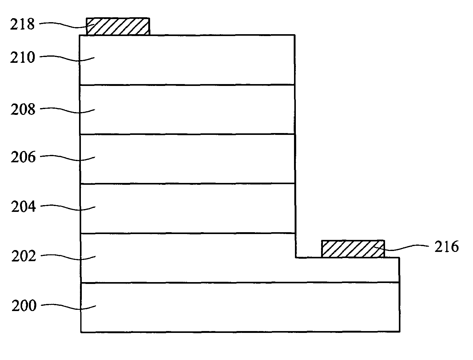
[0018]The present invention discloses a method for manufacturing a light-emitting diode, in which only two masks are employed, such that the process time can be effectively shortened to increase the throughput, the cost can be decreased, and the yield can be greatly enhanced. In order to make the illustration of the present invention more explicit and complete, the following description is stated with reference to FIGS. 2a to 2i.

[0019]FIGS. 2a to 2i are schematic flow diagrams showing the process for manufacturing a light-emitting diode in accordance with a preferred embodiment of the present invention. When the method of the present invention is used to manufacture a light-emitting diode, a substrate 200 is firstly provided, in which the substrate 200 is preferably composed of, for example, sapphire, SiC, ZnO, Si, GaP, GaAs, Al2O3 or other suitable substrate materials. A first conductivity type cladding layer 202, an active layer 204 and a second conductivity type cladding layer 2...


PUM


Abstract

A method for manufacturing a light-emitting diode (LED) is disclosed. In the method, a substrate is firstly provided, in which a first conductivity type cladding layer, an active layer, a second conductivity type cladding layer, a superlattice contact layer and a transparent conductive oxide layer are stacked on the substrate in sequence. Next, an etching mask layer is formed on a portion of the transparent conductive oxide layer, in which the etching mask layer is an insulator. Then, a definition step is performed by using the etching mask layer to remove an exposed portion of the transparent conductive oxide layer, and the superlattice contact layer, the second conductivity type cladding layer and the active layer under the exposed portion of the transparent conductive oxide layer until the first conductivity type cladding layer is exposed. The etching mask layer is then removed. Subsequently, a first conductivity type electrode is formed on the exposed portion of the first conductivity type cladding layer, and a second conductivity type electrode is formed on the transparent conductive oxide layer.

Description

RELATED APPLICATIONS[0001]The present application is based on, and claims priority from, Taiwan Application Serial Number 94106119, filed Mar. 1, 2005, the disclosure of which is hereby incorporated by reference herein in its entirety.FIELD OF THE INVENTION[0002]The present invention relates to a method for manufacturing a light-emitting diode (LED), and more particularly, to a method for manufacturing a light-emitting diode, in which the process can be simplified.BACKGROUND OF THE INVENTION[0003]FIGS. 1a to 1n are schematic flow diagrams showing the process for manufacturing a conventional light-emitting diode. Conventionally, in the fabrication of the light-emitting diode, a substrate 100 is firstly provided, in which the substrate 100 is a sapphire substrate, for example. Next, an N-type cladding layer 102, an active layer 104 for illuminating and a P-type cladding layer 106 are grown on the substrate 100 in sequence by an epitaxial method, in which a material of the N-type cladd...

Claims


Application Information

Patent Timeline
Patent Type & Authority Patents(United States)
IPC IPC(8): H01L21/00H01L33/04H01L33/42
CPCB82Y20/00H01L33/04H01L33/42
Inventor SHEI, SHIH-CHANGLEE, MING-LUM
Owner EPISTAR CORP
Why Eureka
Try Eureka