

LED with current confinement structure and surface roughening
a current confinement and surface roughening technology, applied in the field of light-emitting diodes, can solve the problems of limited external quantum efficiency, and achieve the effect of enhancing light extraction features
- Summary
- Abstract
- Description
- Claims
- Application Information
AI Technical Summary
Benefits of technology
Problems solved by technology
Method used
Image

Examples
Embodiment Construction
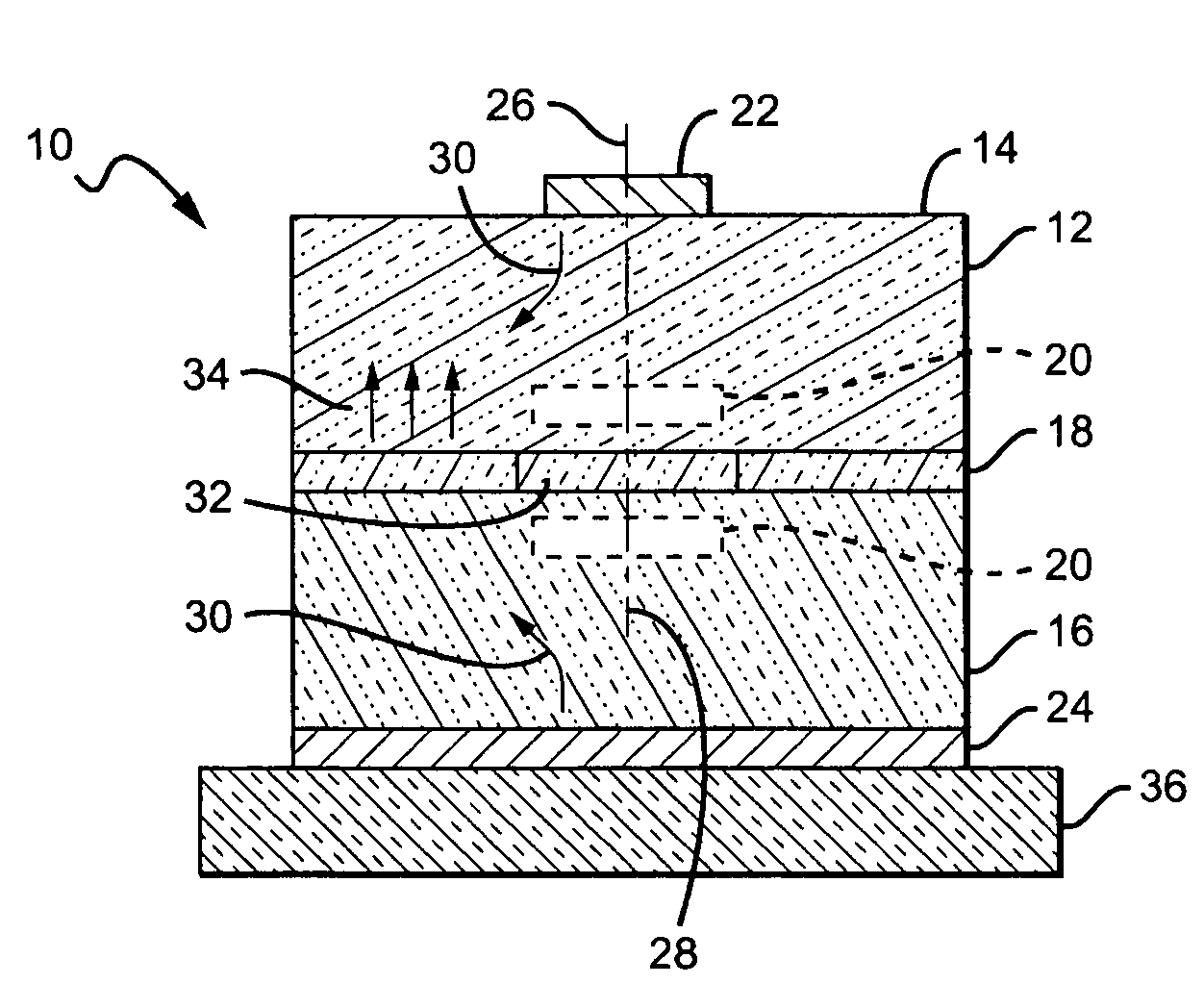
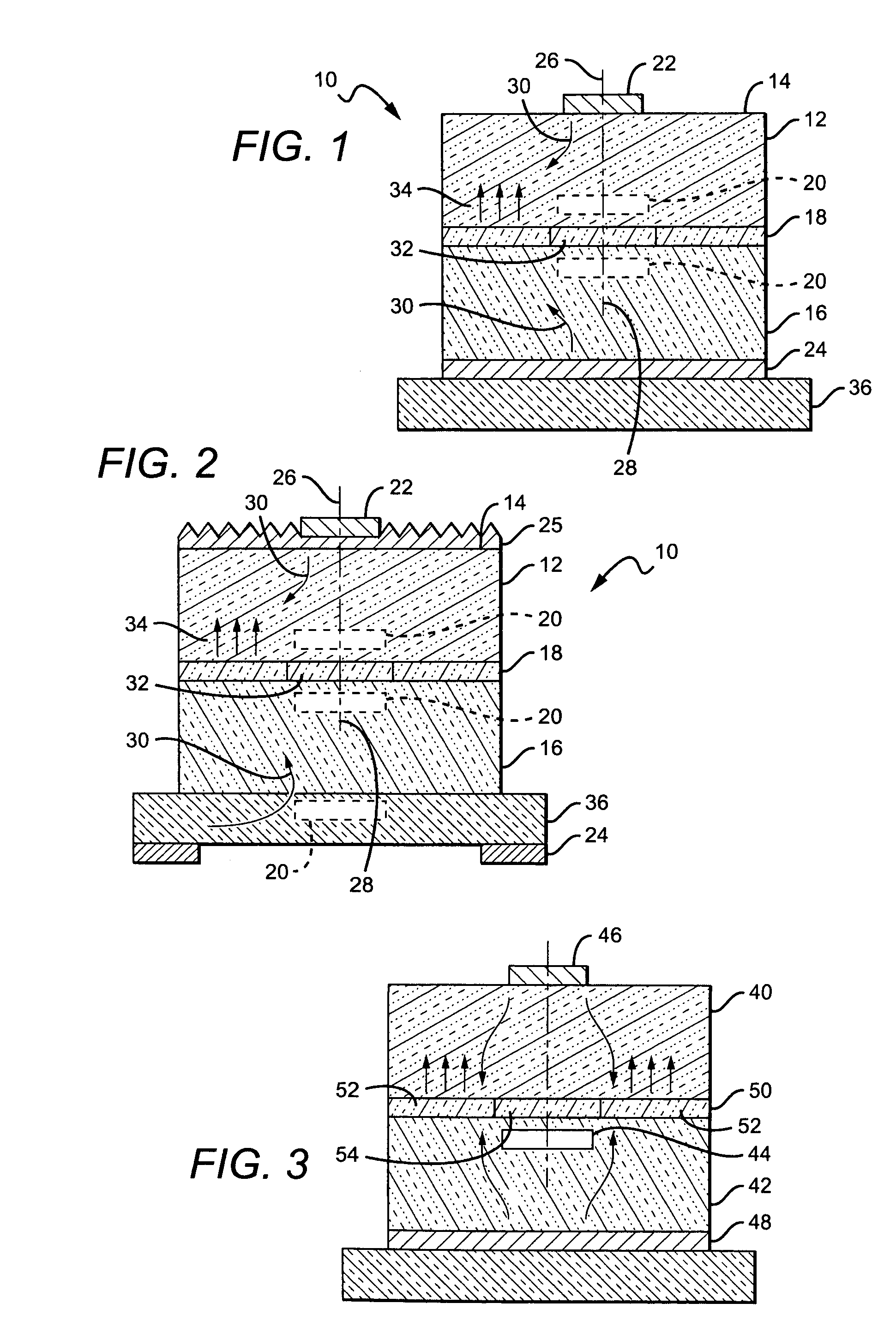
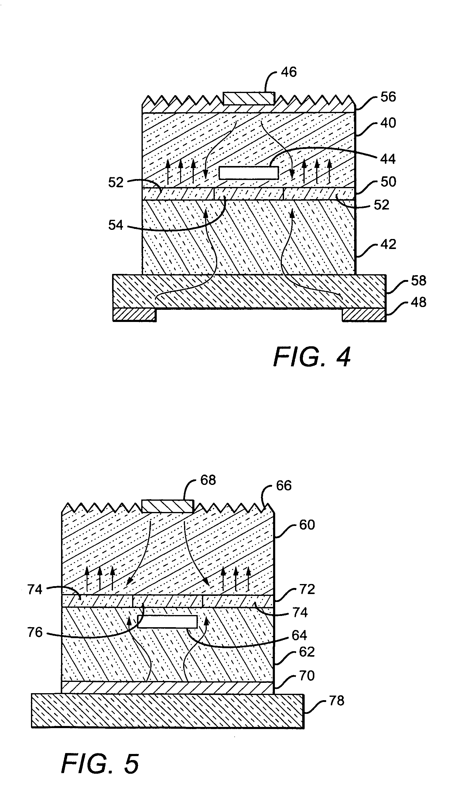
[0022]The present invention provides improved light extraction for light emitting diodes (LEDs) through a confinement structure that is formed within at least one of the p-type layer of material and the n-type layer of material of a base LED structure. The confinement structure is generally aligned with the contact on the top and primary emission surface of the LED and substantially prevents the emission of light from the area of the active region that is coincident with the area of the confinement structure and the top-surface contact. Thus, light that would otherwise emit under and be absorbed by the top-surface contact is redirected to other regions of the active layer and the emitting side where the absorbing affect of the contact is substantially reduced. In a preferred embodiment, the current confinement structure is formed within the base LED structure using ion implantation. The current confinement structure may also be formed in the LED base structure using selective oxidat...
PUM
 Abstract
Description
Claims
Application Information