Integration of fault detection with run-to-run control

Inactive Publication Date: 2008-02-26
APPLIED MATERIALS INC
View PDF436 Cites 62 Cited by
  • Summary
  • Abstract
  • Description
  • Claims
  • Application Information

AI Technical Summary

Benefits of technology

[0012]The present invention addresses the problems described above by integrating run-to-run and fault detection techniques. Specifically, semiconductor wafers and other items are processed in conjunction with a manufacturing execution system using a run-to-run controller and a fault detection system. Initially, and in accordance with one more embodiments of the present invention, a recipe is received from the manufacturing execution system by the run-to-run controller for controlling a tool. This recipe includes a setpoint for obtaining one or more

Problems solved by technology

With many of the quality checks, the measurements can only be made after the wafers have undergone processing operations subsequent to those responsible for producing the aberrations.
Furthermore, a period of time and a number of process steps typically pass between the introduction of the aberration and their detection.
As a result, worn polishing pads inevitably require more time than new pads to produce a desired thickness.
While run-to-run control may be used to address process drifts, it is inadequate for situations where a tool is simply no longer capable of producing an acceptable product, regardless of adjustments made to the recipe setpoints.
Similarly, run-to run control does not address situations where a wafer contains a flaw.
These situations are termed tool or wafer property faults.
A tool th

Method used


Image

  • Integration of fault detection with run-to-run control
  • Integration of fault detection with run-to-run control
  • Integration of fault detection with run-to-run control

Examples


Embodiment Construction

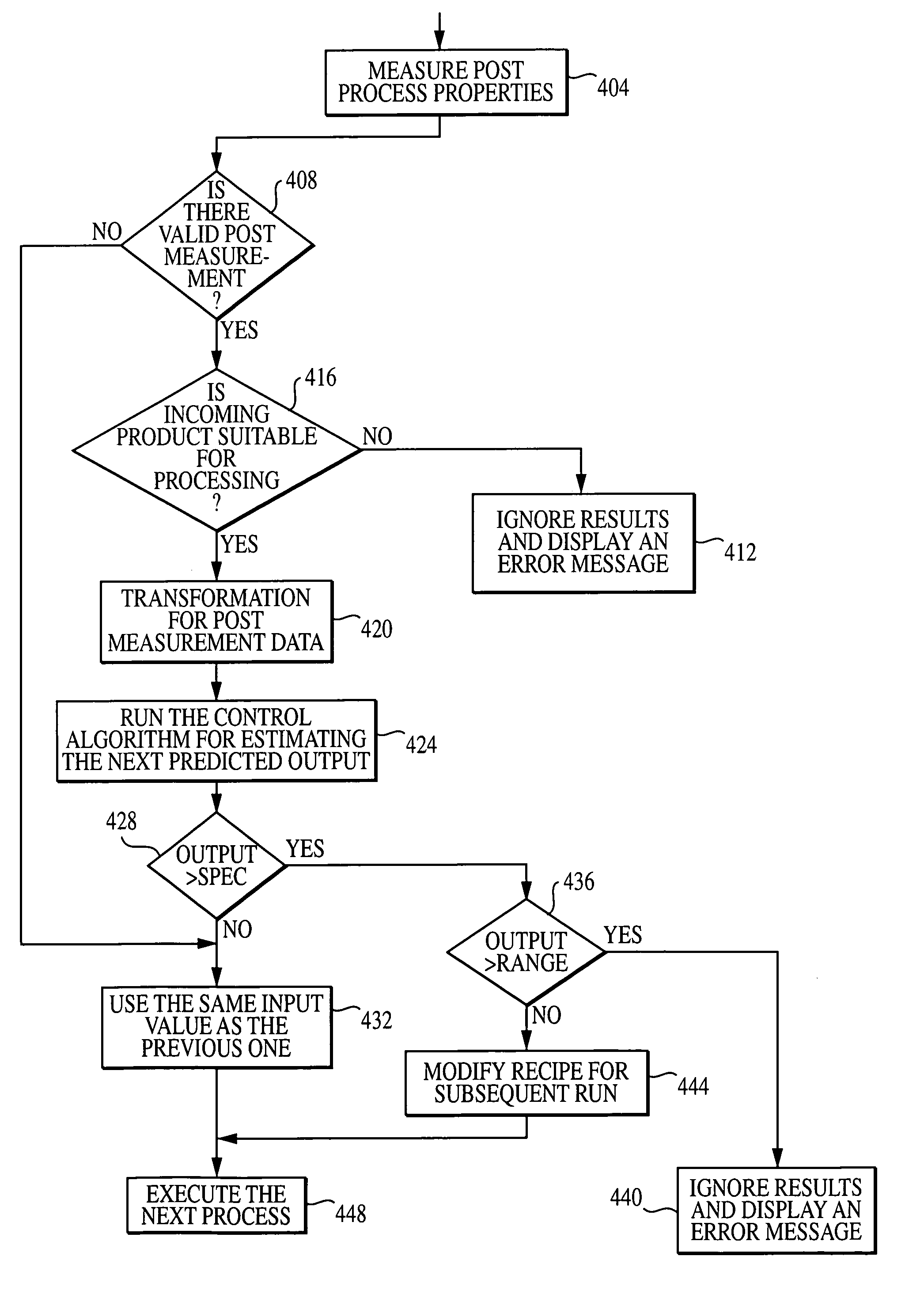
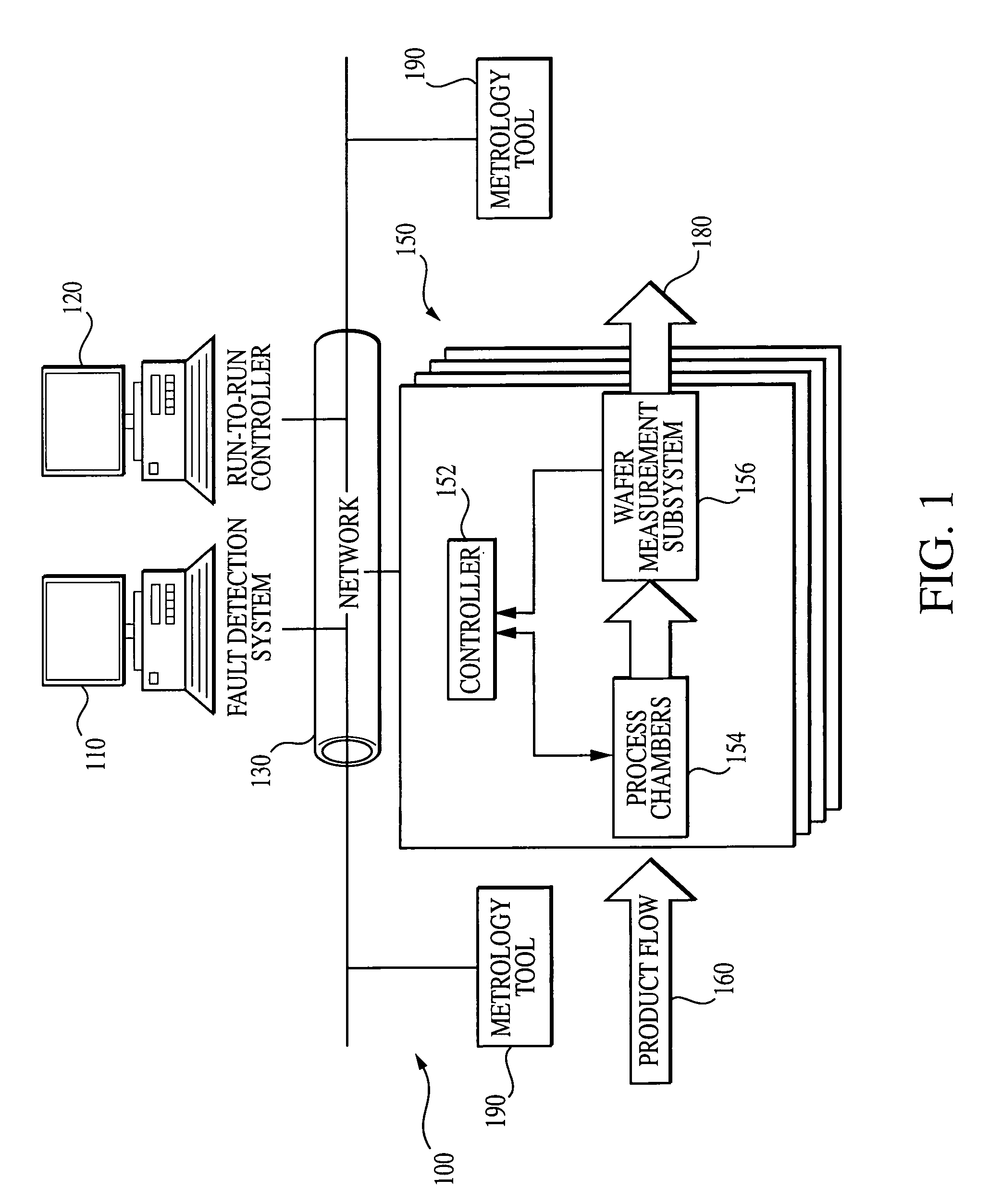
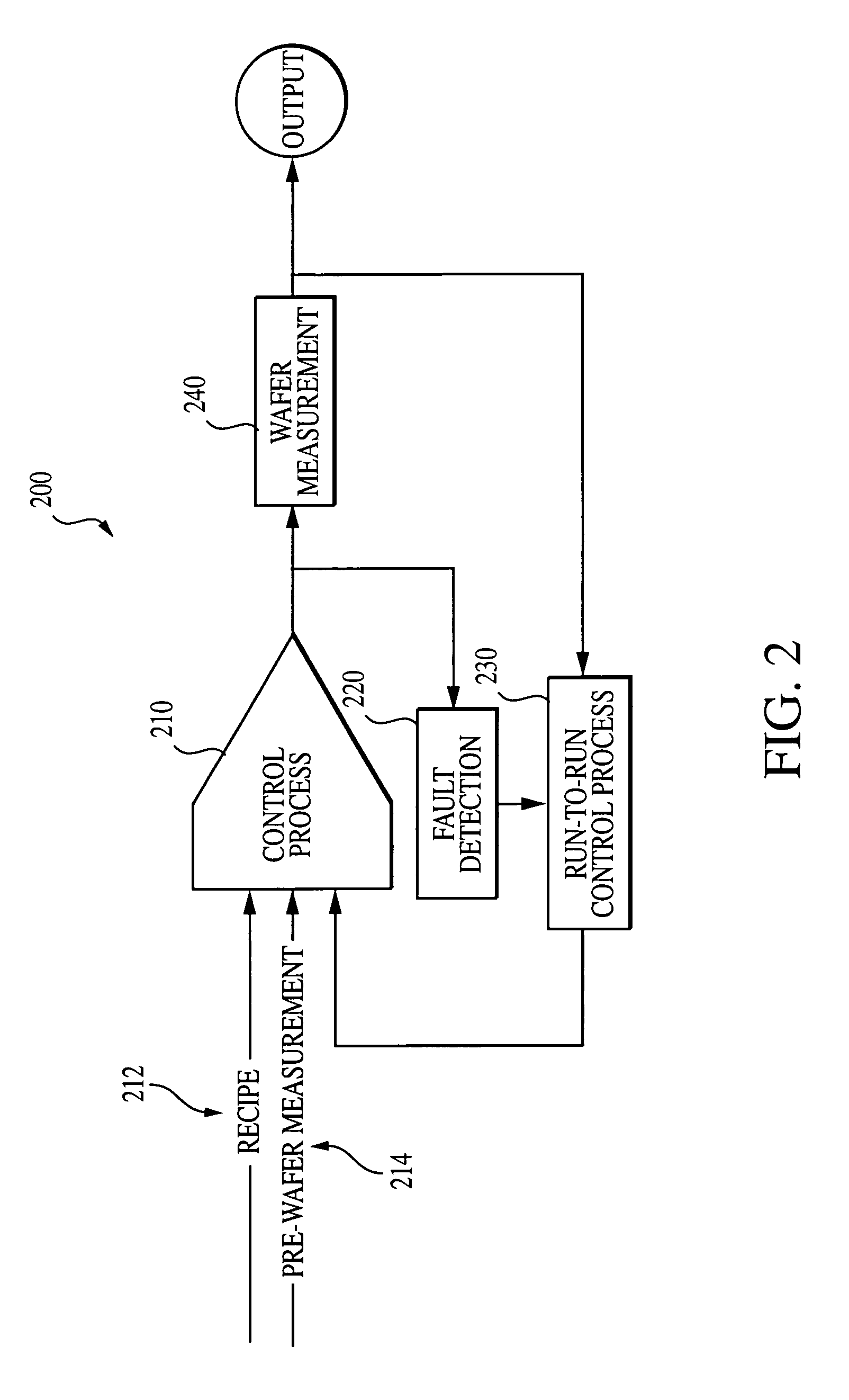
[0024]In accordance with one or more embodiments of the present invention, a technique is provided for processing semiconductor wafers in conjunction with a manufacturing execution system using a run-to-run controller and a fault detection system. More particularly, the manufacturing execution system transfers a recipe to the run-to-run controller for controlling a tool. This recipe includes a setpoint for obtaining one or more target wafer properties. In addition, the fault detection system monitors processing of the wafers by measuring processing attributes including fault conditions and wafer properties. The run-to-run controller modifies the setpoints of the recipe according to the processing attributes (received from the fault detection system as well as e.g., other information gathering sources) to maintain the target wafer properties, except in cases when a fault condition is detected by the fault detection system.

[0025]FIG. 1 depicts at least one example of a hardware block ...


PUM


Abstract

Semiconductor wafers are processed in conjunction with a manufacturing execution system using a run-to-run controller and a fault detection system. A recipe is received from the manufacturing execution system by the run-to-run controller for controlling a tool. The recipe includes a setpoint for obtaining one or more target wafer properties. Processing of the wafers is monitored by measuring processing attributes including fault conditions and wafer properties using the fault detection system and one or more sensors. Setpoints of the recipe may be modified at the run-to-run controller according to the processing attributes to maintain the target wafer properties, except in cases when a fault condition is detected by the fault detection system. Thus, data acquired in the presence of tool or wafer fault conditions are not used for feedback purposes. In addition, fault detection models may be used to define a range of conditions indicative of a fault condition. In these cases, the fault detection models may be modified to incorporate, as parameters, setpoints of a recipe modified by a run-to-run controller.

Description

CROSS REFERENCE TO RELATED APPLICATION[0001]This application claims the benefit of U.S. Provisional Application No. 60 / 305,140 filed on Jul. 16, 2001, which is incorporated herein by reference.FIELD OF THE INVENTION[0002]The present invention relates generally to semiconductor manufacture. More particularly, the present invention relates to techniques for manufacturing semiconductors by integrating fault detection concepts with run-to-run control.BACKGROUND OF THE INVENTION[0003]In typical semiconductor manufacturing processes, semiconductor wafers, or simply wafers, are advanced through a number of stations within what is referred to as a fab. At each location in this assembly line-like process, processing equipment or tools perform processing operations to modify the wafers. For example, one tool may add various layers onto the wafers (e.g., a deposition tool) while another may modify the layers (e.g., etching tools) to form a completed semiconductor product.[0004]As they are move...

Claims


Application Information

Patent Timeline
IPC IPC(8): G06F19/00H05B1/02G05B11/01H01L21/02G05B19/418G05B23/02H01L21/00H01L21/66
CPCG05B19/41865G05B23/0286G05B2219/31357G05B2219/31443G05B2219/45031Y02P90/02H01L21/00G05B19/418
Inventor REISS, TERRY P.SHANMUGASUNDRAM, ARULKUMAR P.SCHWARM, ALEXANDER T.
Owner APPLIED MATERIALS INC
Why Eureka
Try Eureka