Transflective liquid crystal display with fringing and longitudinal electric field
a transflective liquid crystal display and longitudinal electric field technology, applied in non-linear optics, instruments, optics, etc., can solve the problems of inapplicability under low light levels or dark ambient conditions, easy washed out image of transmissive liquid crystal display, and relatively high power consumption, so as to simplify the manufacturing process and reduce the manufacturing cost
- Summary
- Abstract
- Description
- Claims
- Application Information
AI Technical Summary
Benefits of technology
Problems solved by technology
Method used
Image
Examples
embodiment 1
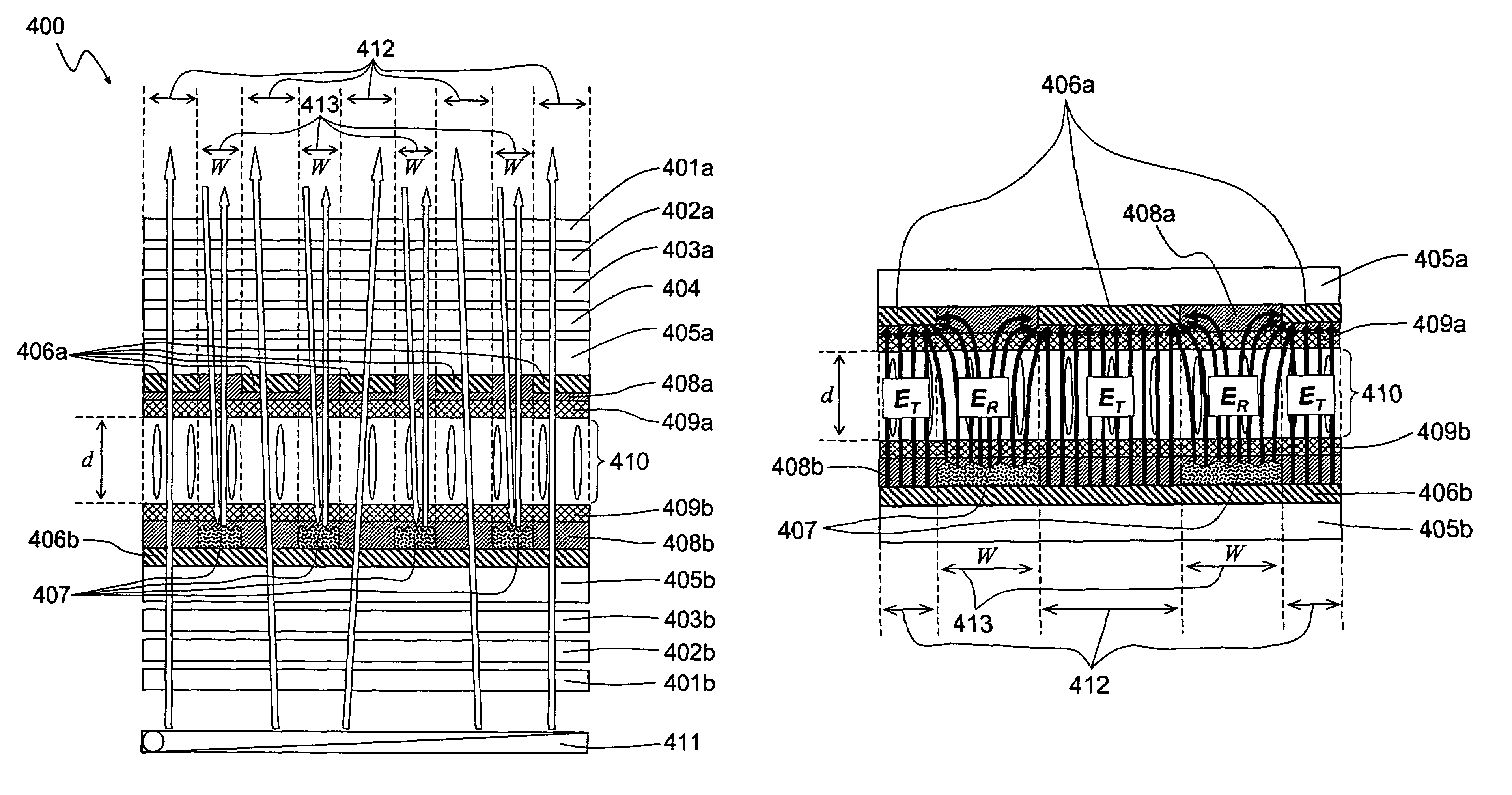
[0050]FIG. 4 shows the structure of a first embodiment of the transflective LCD 400 with uniform cell gap configuration of the present invention which consists of a first transparent substrate 405 a coated with a patterned ITO layer 406a, a first non-conductive planar layer 408a, and a first vertical alignment film 409a; a second transparent substrate 405b coated with a non-patterned ITO layer 406b, a patterned reflector 407, a second non-conductive planar layer 408b, and a second vertical alignment film 409b; and a vertically aligned negative dielectric anisotropic nematic liquid crystal layer 410 with thickness d sandwiched between the first vertical alignment film 409a and the second vertical alignment film 409b.
[0051]A negative birefringence c-film 404, a first quarter-wave retardation film 403a, a first half-wave retardation film 402a, and a first polarizer 401a are further laminated on the outer surface of the first substrate 405a, wherein the negative birefringence c-film 40...
second embodiment
[0060]In the first embodiment, the common electrode pattern on the first substrate is mutually complementary with the reflector pattern on the second substrate; therefore, the first substrate aligns with the second substrate. To avoid that alignment requirement, FIG. 10 shows the schematic structure according to the second embodiment of the transflective LCD 900 with uniform cell gap configuration according to the present invention. The structure in the second embodiment includes a first transparent substrate 905a coated with a non-patterned ITO layer 906a and a first vertical alignment film 909a, a second transparent substrate 905b coated with a patterned ITO layer 906b, a patterned reflector 907, a non-conductive planar layer 908, and a second vertical alignment film 909b, a vertically aligned negative dielectric anisotropic nematic liquid crystal layer 910 with thickness d sandwiched between the first vertical alignment film 909a and the second vertical alignment film 909b. A neg...
PUM
| Property | Measurement | Unit |
|---|---|---|
| cell gap d | aaaaa | aaaaa |
| crystal pretilt angles | aaaaa | aaaaa |
| width W | aaaaa | aaaaa |
Abstract
Description
Claims
Application Information


