Method and apparatus of temperature compensation for integrated circuit chip using on-chip sensor and computation means

a technology of integrated circuits and sensors, applied in the field of temperature compensation integrated circuits, can solve the problems of expensive procedures for calibrating integrated circuits (ic) at two or more temperatures, test equipment and test logistics, etc., and achieve the effects of simple test logistics, reduced total test time, and reduced temperature dri

Active Publication Date: 2008-03-04
ATMEL CORP
View PDF18 Cites 13 Cited by
  • Summary
  • Abstract
  • Description
  • Claims
  • Application Information

AI Technical Summary

Benefits of technology

[0008]Briefly, the present invention achieves a very low temperature drift without adding test costs by running a high accuracy, high quality IC testing through at least two independent test sites using an on-chip reference circuit and temperature sensor (or other sensor for other drift measurements) with on-chip evaluation circuits and programming in cooperation with an external reference. The programming is a two-step algorithm stored in non-volatile memory that makes it possible to split the calibration steps at two completely independent sites. The first, initial integrated system on-chip calibration test of a condition, such as a reference voltage, is performed at a factory site, at a relatively high temperature (for instance, at 85° C.), before the integrated system on-chip is shipped to the customer. The initial calibration factory test data is stored in a non-volatile memory on the integrated system on-chip itself. On the other hand, the second integrated system on-chip calibration test is performed at a customers's site, at a local temperature (for instance, 30° C.), that is typically much lower than the first test site relatively high temperature. The customer supplies an external reference voltage source residing on the integrated system on-chip, and the second calibration test of the supplied voltage reference is performed by the integrated system on-chip itself by running the second calibration algorithm stored internally in the integrated system on-chip using test data stored in the non-volatile memory from the first calibration test. Thus, all necessary circuitry for running calibration algorithms is integrated on the chip itself, including a CPU or dedicated logic and associated circuits, or by dedicated logic. A CPU and associated circuits could be shared with other functionality of the chip. Thus, the present invention reduces the test equipment requirements by splitting the calibration steps between at least two completely independent test sites. One aspect of the present invention is directed to an apparatus for temperature calibration of an internal reference source residing on an integrated system on-chip using a temperature sensor that is on-chip. Other calibrations, such as frequency calibrations, could be carried out in the same way, with a frequency sensor carried on-chip.
[0045]The invention has the following advantages: Reduced total test time because both sites will run its own tests independently of the calibration requirement. A chip manufacturer very often performs its packaged part test at high temperature, and the system manufacturer performs its tests typically at room temperature. By exploiting this fact, the chipmaker does not need to have an expensive second test insertion at room temperature only for calibration reasons.
[0046]A system manufacturer can optimize the algorithm to its own needs. For instance, with a band-gap gap voltage reference, the temperature coefficient may be zero at a certain temperature and temperature drift will increase when moving away from this temperature. With the present invention, the calibration algorithm can be extended to minimize the temperature drift in different temperature ranges selected by the system manufacturer.
[0047]Simple test logistics and reduced costs occur because the chip itself keeps track of all necessary calibration data and the correct calibration algorithm is built into the chip.

Problems solved by technology

However, calibrating an integrated circuit (IC) at two or more temperatures is an expensive procedure in terms of test time, test equipment and test logistics.

Method used


Image

  • Method and apparatus of temperature compensation for integrated circuit chip using on-chip sensor and computation means
  • Method and apparatus of temperature compensation for integrated circuit chip using on-chip sensor and computation means
  • Method and apparatus of temperature compensation for integrated circuit chip using on-chip sensor and computation means

Examples


Embodiment Construction

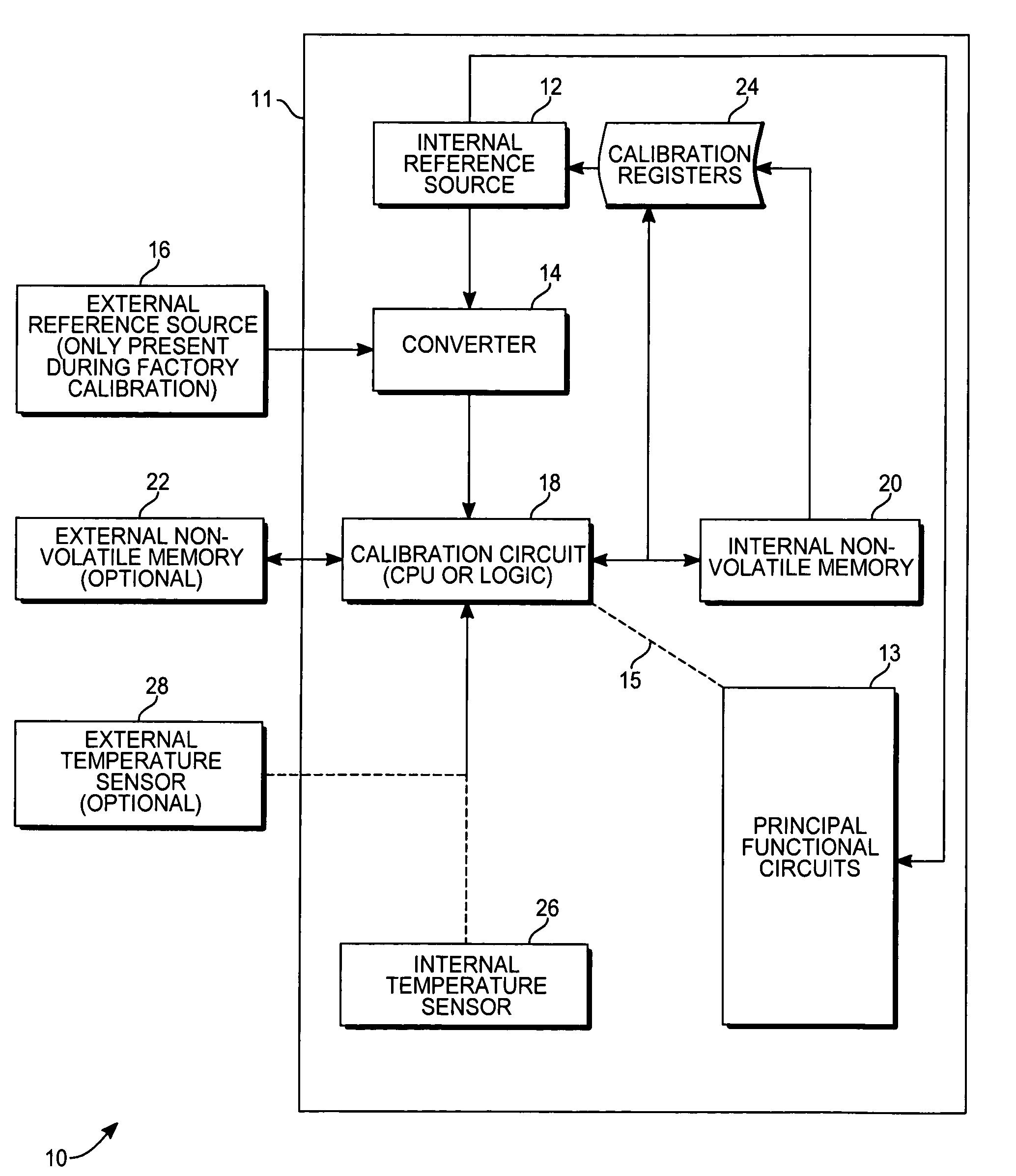
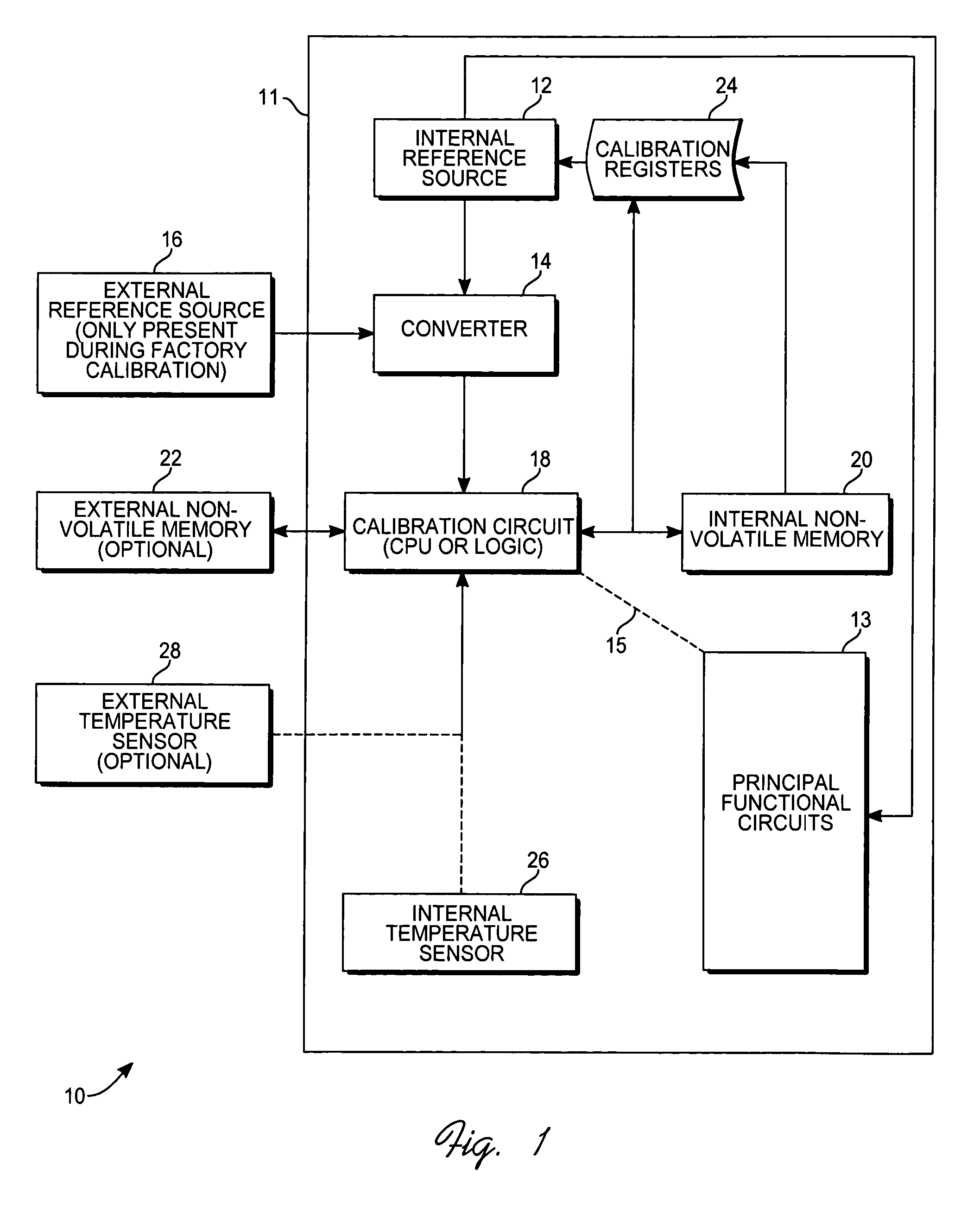
[0058]FIG. 1 depicts an apparatus 10 for temperature calibration of an internal reference source residing on an integrated system on the integrated circuit chip 11. The calibration method of the present invention is aimed to improve the temperature stability of the integrated system with an internal reference source 12 and an internal sensor 26. By integrated system here we mean a true system on-chip design, or a system with more than one chip integrated in the same package.

[0059]A converter 14 is coupled to the internal reference source 12. Converter 14 is a generic converter that converts the reference value to a digital value. In a case of an internal analog voltage reference, the converter is an analog-to-digital converter (ADC). In a case of an internal time reference, i.e. an oscillator, the converter is a time counter. The internal reference source is calibrated with respect to some parameter, such as temperature, measured by an on-chip sensor, such as a temperature variable ...


PUM

PropertyMeasurementUnit
temperatureaaaaaaaaaa
sink currentsaaaaaaaaaa
band-gap voltageaaaaaaaaaa

Abstract

A method and apparatus of temperature compensation for an integrated circuit using on-chip circuits, sensors, and an algorithm. The chip includes an on-chip reference circuit, an on-chip sensor measuring a parameter relative to the reference, and an on-chip computation means for processing an algorithm. A supplemental off-chip reference circuit is also used. The algorithm carries out the following steps: (A) performing a first calibration of an internal reference residing in an integrated circuit system on-chip at a first (higher) temperature at a first testing site, and (B) utilizing calibration data obtained at the step (A) to perform a second calibration of the internal reference source residing on the integrated system on-chip at a second (lower) temperature at a second testing site.

Description

TECHNICAL FIELD[0001]The present invention relates to temperature compensated integrated circuits.BACKGROUND ART[0002]Prior art temperature compensated integrated circuits (IC) are used mostly in the battery management systems. U.S. Pat. No. 5,955,869 discloses a method for monitoring remaining capacity of a battery pack. There are two different procedures that are used to estimate the battery pack remaining capacity. In a first procedure, data is generated on the battery pack to estimate remaining battery capacity; and in the second procedure, data transmitted to the battery pack from a host device is used to estimate remaining battery capacity. The battery pack switches between these two procedures. For example, the battery pack switches from the first procedure to the second procedure when the battery current falls below a threshold value.[0003]More specifically, the '869 patent discloses a smart battery device installed in a host computer that optimizes the performance of the re...

Claims


Application Information

Patent Timeline
Patent Type & Authority Patents(United States)
IPC IPC(8): G01K7/00G01R35/00
CPCG01R35/005
Inventor AAS, ARNEGANGSTO, GUNNAR
Owner ATMEL CORP
Why Eureka
Try Eureka