Ferromagnetic liner for conductive lines of magnetic memory cells and methods of manufacturing thereof

a technology of magnetic memory cells and conductive lines, which is applied in the direction of digital storage, semiconductor devices, instruments, etc., to achieve the effect of reducing the current and power consumption of an mram device, and increasing the flux concentration of conductive lines

Inactive Publication Date: 2008-03-18
IBM CORP +1
View PDF9 Cites 14 Cited by
  • Summary
  • Abstract
  • Description
  • Claims
  • Application Information

AI Technical Summary

Benefits of technology

[0007]Embodiments of the present invention achieve technical advantages by providing methods of forming ferromagnetic liners around wordlines or bitlines of an MRAM device.
[0010]Advantages of embodiments of the present invention include providing improved methods of forming ferromagnetic liners around conductive lines of MRAM devices. The write current and the power consumption of an MRAM device can be reduced in accordance with embodiments of the present invention. The ferromagnetic liners concentrate or focus the magnetic flux of current run through the conductive lines. In one embodiment, the flux concentration of conductive lines is further increased by the formation of in-bound poles of ferromagnetic material proximate the bottom edges of the conductive lines.

Problems solved by technology

Because MRAM devices operate differently than traditional memory devices and because they are relatively new, they introduce design and manufacturing challenges.

Method used


Image

  • Ferromagnetic liner for conductive lines of magnetic memory cells and methods of manufacturing thereof
  • Ferromagnetic liner for conductive lines of magnetic memory cells and methods of manufacturing thereof
  • Ferromagnetic liner for conductive lines of magnetic memory cells and methods of manufacturing thereof

Examples


Embodiment Construction

[0019]The making and using of the presently preferred embodiments are discussed in detail below. It should be appreciated, however, that the present invention provides many applicable inventive concepts that can be embodied in a wide variety of specific contexts. The specific embodiments discussed are merely illustrative of specific ways to make and use the invention, and do not limit the scope of the invention.

[0020]The present invention will be described with respect to preferred embodiments in a specific context, namely an MRAM device. Embodiments of the present invention may also be applied, however, to other magnetic devices, namely, magnetic memory devices, for example.

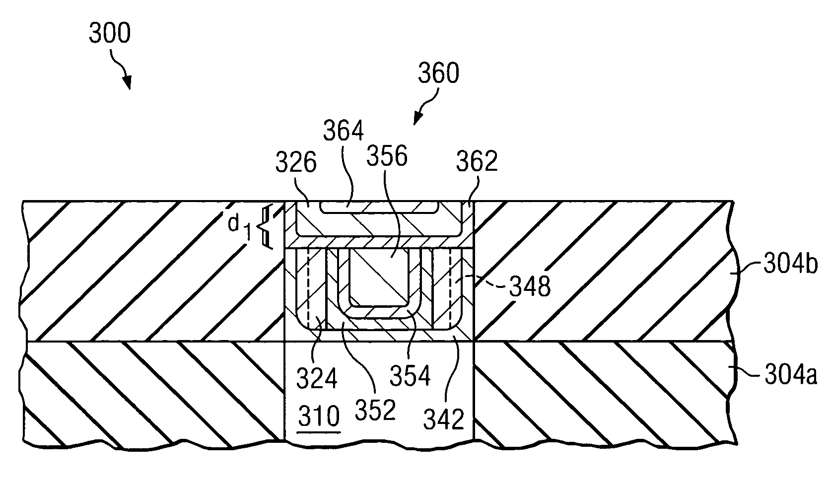
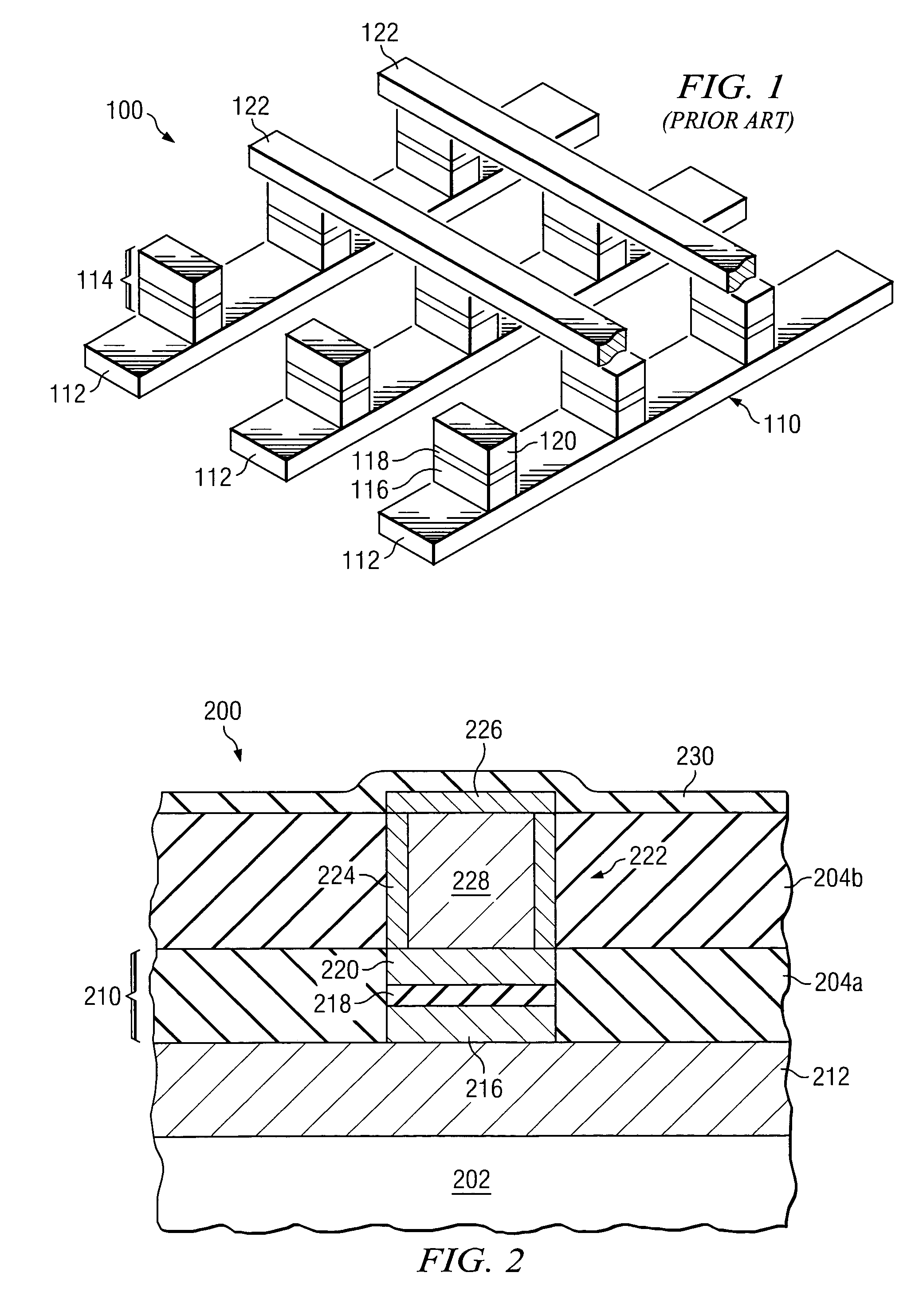
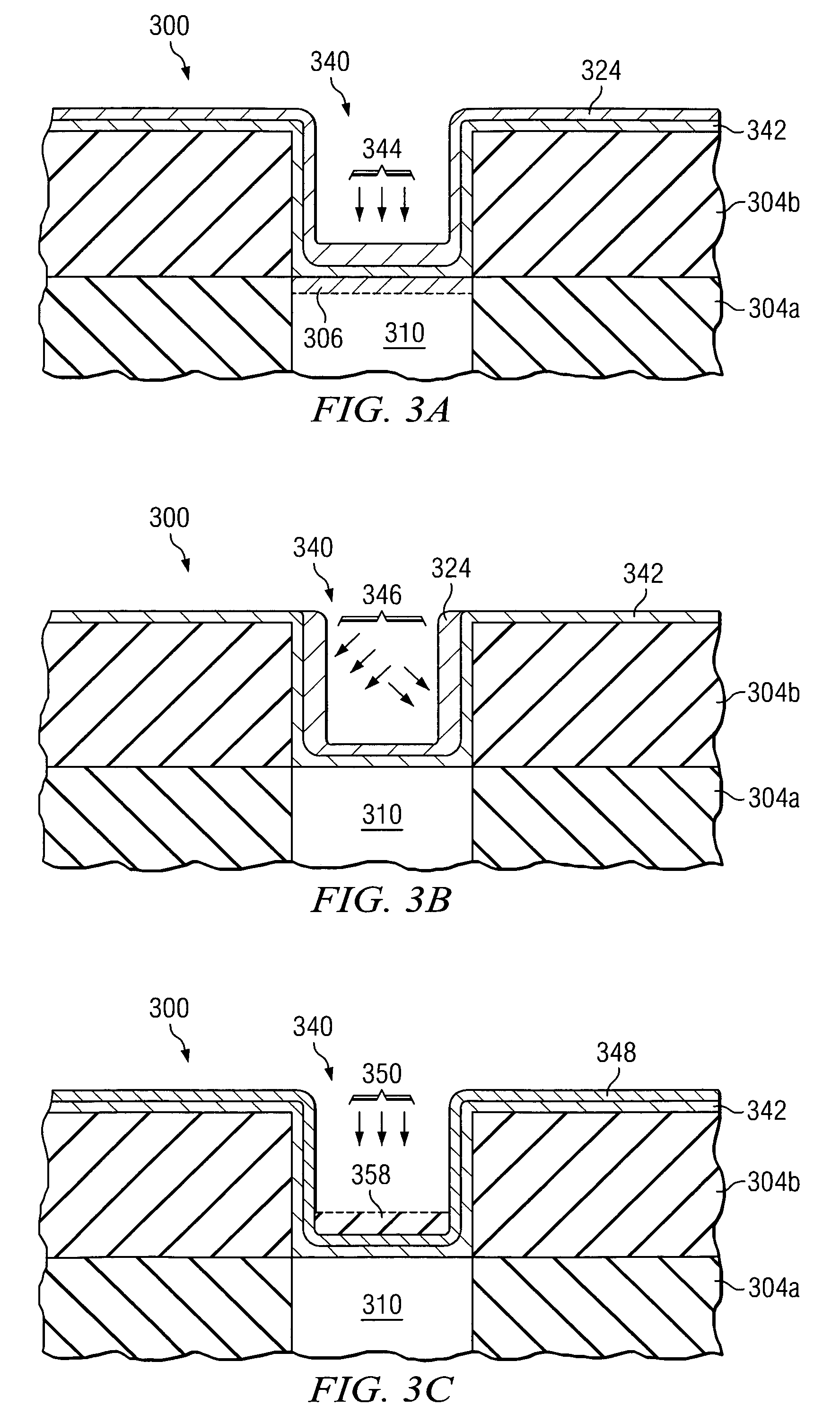
[0021]FIG. 1 illustrates a perspective view of a prior art crosspoint MRAM 100 device having bitlines 112 located substantially perpendicular to wordlines 122 in adjacent metallization layers. Magnetic stacks 114 are positioned between the bitlines 112 and wordlines 122 adjacent and electrically coupled to bitli...


PUM


Abstract

Methods of forming ferromagnetic liners on the top surface and sidewalls of conductive lines of magnetic memory devices. The ferromagnetic liners increase the flux concentration of current run through the conductive lines, reducing the amount of write current needed to switch magnetic memory cells. In one embodiment, an in-bound pole is formed at the bottom edge of conductive lines, further concentrating the flux.

Description

TECHNICAL FIELD[0001]The present invention relates generally to the fabrication of semiconductor devices, and more particularly to the fabrication of magnetic memory devices.BACKGROUND[0002]Semiconductors are used in integrated circuits for electronic applications, including radios, televisions, cell phones, and personal computing devices, as examples. One type of semiconductor device is a semiconductor storage device, such as a dynamic random access memory (DRAM) and flash memory, which use a charge to store information.[0003]A recent development in semiconductor memory devices involves spin electronics, which combines semiconductor technology and magnetics. The spin of electrons, rather than the charge, is used to indicate the presence of binary states “1” and “0.” One such spin electronic device is a magnetic random access memory (MRAM) device, which includes conductive lines (wordlines and bitlines) positioned in different directions, e.g., perpendicular to one another in differ...

Claims


Application Information

Patent Timeline
Patent Type & Authority Patents(United States)
IPC IPC(8): H01L21/00
CPCG11C11/16H01L21/76844H01L21/76846H01L21/76849H01L21/76874H01L27/222H10B61/00
Inventor LEUSCHNER, RAINERRABERG, WOLFGANGBROWN, STEPHEN L.FINDEIS, FRANKKANAKASABAPATHY, SIVANANDHA K.VIETH, MICHAEL
Owner IBM CORP
Why Eureka
Try Eureka