Apparatus and method for controlling the beam current of a charged particle beam

a charged particle and beam current technology, applied in the direction of heat measurement, particle separator tube details, instruments, etc., can solve the problems of too slow to deliver the throughput needed in large-scale manufacturing, cd or other undesired variations, and the emitter tip is slow, so as to achieve miniaturization and mass production

Active Publication Date: 2008-03-18
ICT INTEGRATED CIRCUIT TESTING GESELLSCHAFT FUER HALBLEITERPRUEFTECHNIK GMBH
View PDF5 Cites 2 Cited by
  • Summary
  • Abstract
  • Description
  • Claims
  • Application Information

AI Technical Summary

Benefits of technology

[0011]The above described apparatus is adapted to switch not only between two but three tip-to-gate voltage levels. The additional mute level needs to be switched only faster than the relatively low scan frequency. Therefore the corresponding voltage swing can be large without causing excessive heat load or in-vacuum power dissipation. Furthermore, the beam current is sufficiently low at the mute level to prevent CD variations due to unwanted exposure doses in regions where the beam spot speed is slow. Also, heat load is reduced since fast switching can be accomplished with a small voltage swing between the write and blank levels. Although the term write level is used, it should be understood that the apparatus according to the aspect of the present invention can also be used for inspecting sample instead of structuring them.
[0013]The tip-to-gate voltage of an emitter tip can be switched very fast by 5 V at a pixel clock frequency, thus leading to a considerable throughput and an acceptable heat load. On the other hand, the 15 V voltage swing between blank and mute levels can be switched slower and heat load or capacitive load are prevented.
[0015]The blank level provides a beam current which is sufficiently low for not writing a pixel at the write scan speed of the beam spot, but high enough so that the voltage swing between the write level and the blank level is relatively small. By this measure, high switching speed and low heat load and power dissipation are achieved during pixel writing. Since the beam current at the blank level is too high for the slow movement of a write scan turn, a mute level of considerably lower beam current is provided. At the mute level, the beam current is so low that even the slow write scan turn does not lead to any CD variations or other undesired results due to the exposure dose by the residual “tip off” current. Accordingly, the aforementioned problems related to CD variation, heat load and power dissipation are avoided or at least reduced.
[0019]Field emission cathodes are advantageous for their capability of miniaturization and mass production. Also, different levels of the beam current can be realized by a relatively simple switching of the tip-to-gate voltage of an individual field emission cathode in an emitter array. Accordingly, the present invention is especially useful in applications where emitter arrays are used. Thus, the above embodiment of the present invention is technically and economically promising.

Problems solved by technology

While electron beam devices can meet the spatial resolution requirements they are often too slow to deliver the throughput needed in large scale manufacturing.
The temporarily integrated exposure dose of the “tip off” current may become too large in the turn regions and lead to variations of the critical dimension (CD) or other undesired results.
This relatively high voltage swing causes the “tip on” / “tip off”switching of emitter tips to be slow and, consequently, limits the throughput.

Method used


Image

  • Apparatus and method for controlling the beam current of a charged particle beam
  • Apparatus and method for controlling the beam current of a charged particle beam
  • Apparatus and method for controlling the beam current of a charged particle beam

Examples


Embodiment Construction

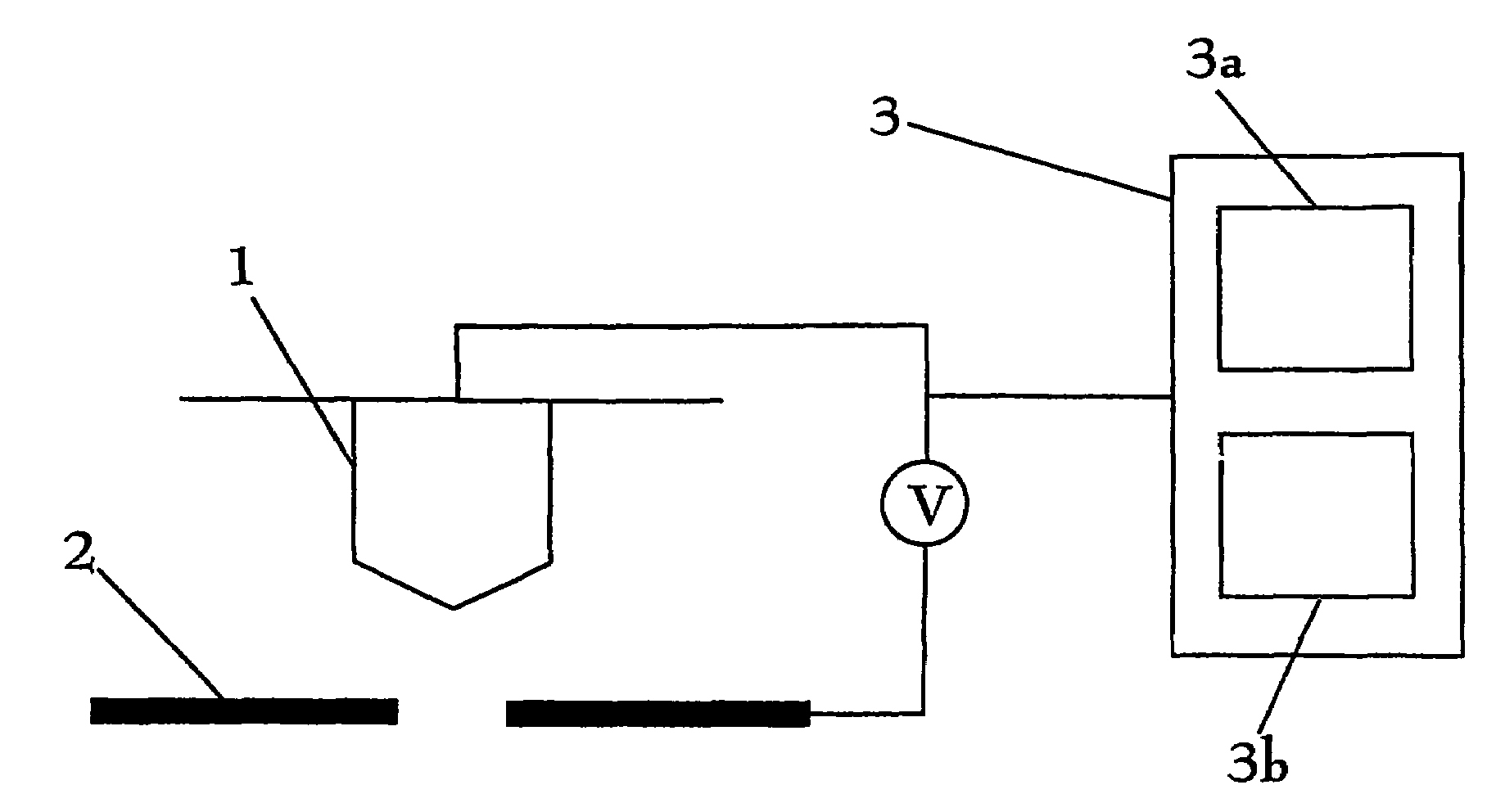
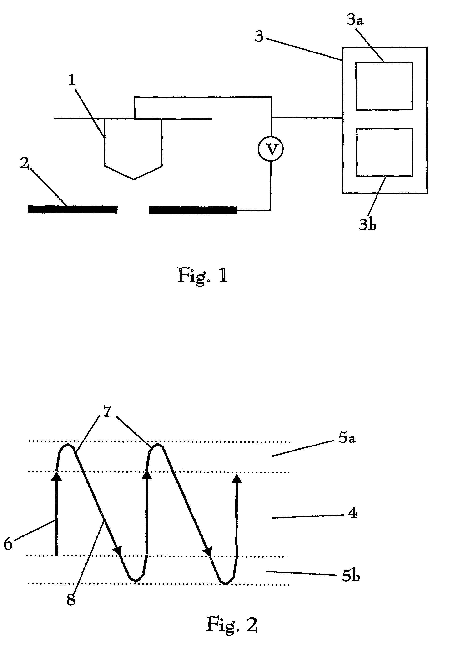
[0024]FIG. 1 is a schematic view of a field emission cathode. Field emission cathodes are known electron beam sources for electron beam devices in applications as diverse as e.g. electron microscopy, electron pattern generators or flat panel displays. They were first proposed by C. A. Spindt (Journal of Appl. Physics, Vol 39 (1968) No. 7, p. 3504-3505). The main elements of the cathode are a very tiny emitter tip 1 and a gate 2. The field emission cathode emits electrons into free space by applying a high electric field to the surface of the emitter tip 1. Without electric field there is usually a potential barrier of theoretically infinite thickness at the interface of the emitter tip and free space or vacuum. The height of the potential barrier depends on the surface material of the emitter tip. When an external electric field is applied to the emitter tip that attracts electrons, the potential barrier thickness reduces. When the electric field at the surface of the emitter tip is...


PUM


Abstract

An apparatus for producing a beam of charged particles is provided, which comprises an emitter (1, 2) and a switching device (3) adapted to switch between first, second and third beam current levels, wherein the beam current at said first current level is suitable for writing a pixel of an image on the surface of a sample, the beam current at said second current level is suitable for not writing a pixel on the surface of said sample, and the beam current at said third current level is lower than the beam current at the second current level. Furthermore, a method of controlling the beam current of a charged particle beam is provided, comprising the steps of switching the beam current of said charged particle beam between first and second current levels, wherein the beam current at said first current level is suitable for writing a pixel of an image on the surface of a sample and the beam current at said second current level is suitable for not writing a pixel on the surface of said sample, and switching the beam current to a third voltage level, wherein the beam current at said third current level is lower than the beam current at the second current level.

Description

FIELD OF THE INVENTION[0001]The present invention relates to an apparatus and a method for controlling the beam current of a charged particle beam, especially for the improved control of the extinction ratio in electron beam apparatus using emitter arrays.BACKGROUND OF THE INVENTION[0002]Technologies like microelectronics, micromechanics and biotechnology have created a high demand in industry for structuring and probing specimens within the nanometer scale. On such a small scale, probing or structuring, e.g. of photomasks, is often done with electron beams which are generated and focused in electron beam devices like electron microscopes or electron beam pattern generators. Electrons beams offer superior spatial resolution compared to e.g. photon beams due to their short wave lengths at a comparable particle energy.[0003]While electron beam devices can meet the spatial resolution requirements they are often too slow to deliver the throughput needed in large scale manufacturing. To ...

Claims


Application Information

Patent Timeline
Patent Type & Authority Patents(United States)
IPC IPC(8): H01J3/14H01J3/02H01J49/08H01J37/24H01J37/302H01J37/304H01J37/317
CPCB82Y10/00B82Y40/00H01J37/243H01J37/3023H01J37/3174H01J2237/06341H01J2237/31774H01J2237/31796
Inventor SELLMAIR, JOSEF
Owner ICT INTEGRATED CIRCUIT TESTING GESELLSCHAFT FUER HALBLEITERPRUEFTECHNIK GMBH
Why Eureka
Try Eureka