Supercharge Your Innovation With Domain-Expert AI Agents!

Data storage circuit

a data storage circuit and data technology, applied in the field of data storage circuits, can solve the problems of disadvantageous increase of the whole area of the data storage circuit, longer access time, and large area of the memory cell, and achieve the effect of reducing standby power consumption

Inactive Publication Date: 2008-03-18
RENESAS ELECTRONICS CORP
View PDF15 Cites 15 Cited by
  • Summary
  • Abstract
  • Description
  • Claims
  • Application Information

AI Technical Summary

Benefits of technology

[0007]It is an object of the present invention to provide a data storage circuit capable of suppressing standby currents in the standby state of a memory cell and reducing standby power consumption.

Problems solved by technology

Since a PMOS has smaller current driving capability than an NMOS, however, there arises a problem that the access time becomes longer.
If the size of the PMOS is made larger in order to maintain the access time, the area of the memory cell becomes larger and the whole area of the data storage circuit disadvantageously increases.

Method used


Image

  • Data storage circuit
  • Data storage circuit
  • Data storage circuit

Examples


Embodiment Construction

[0043]The present invention will be specifically discussed below, referring to figures showing the preferred embodiments.

The First Preferred Embodiment

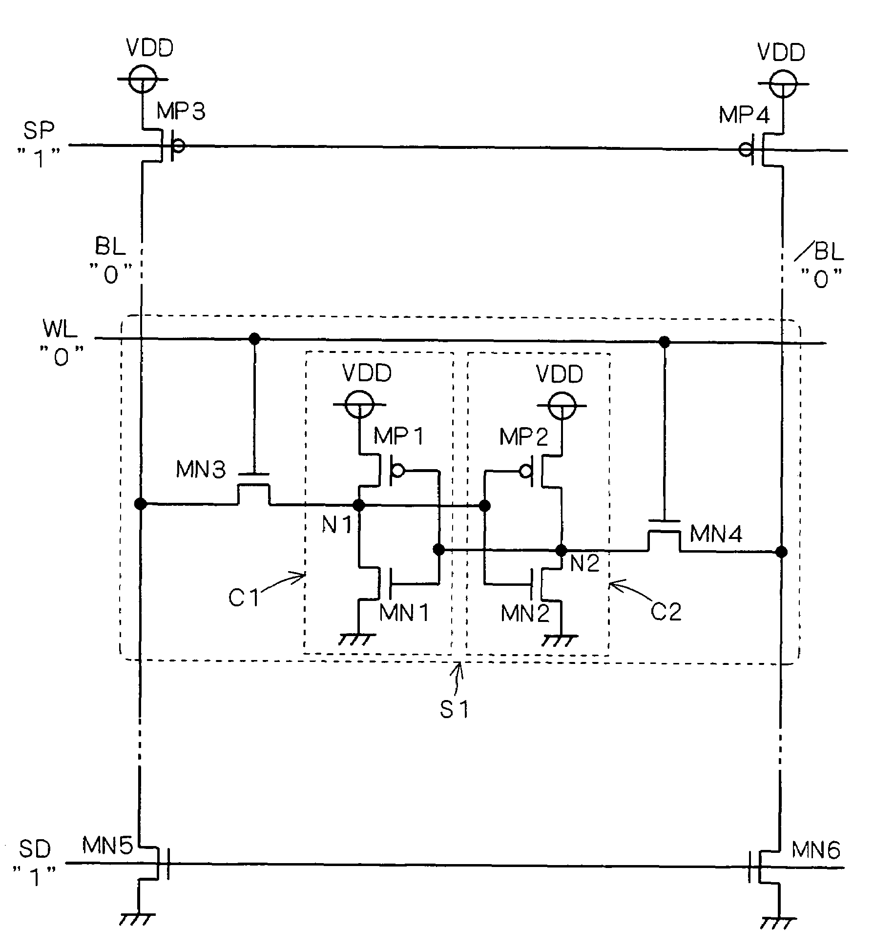
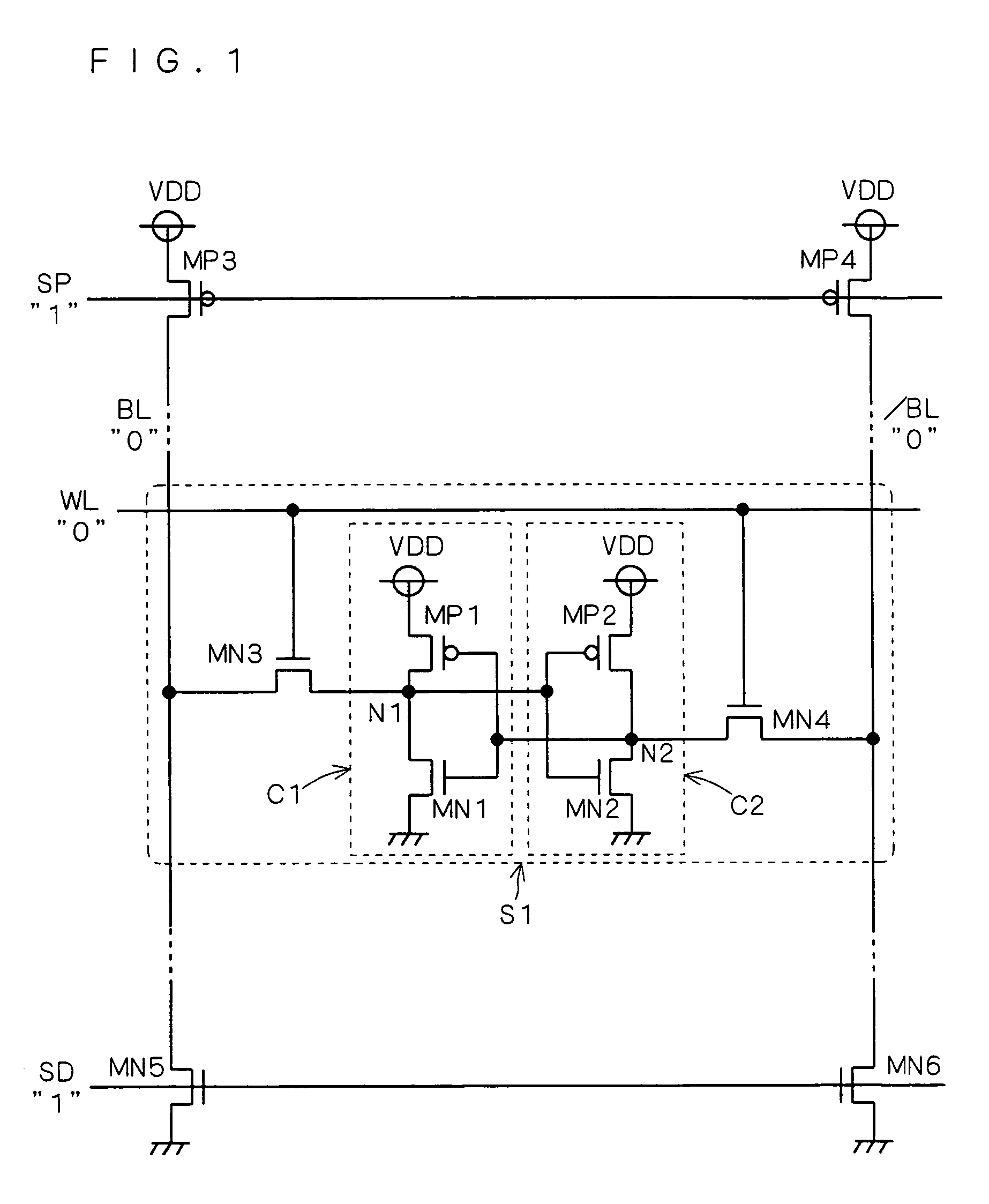
[0044]FIG. 1 shows a configuration of a data storage circuit in accordance with the first preferred embodiment.

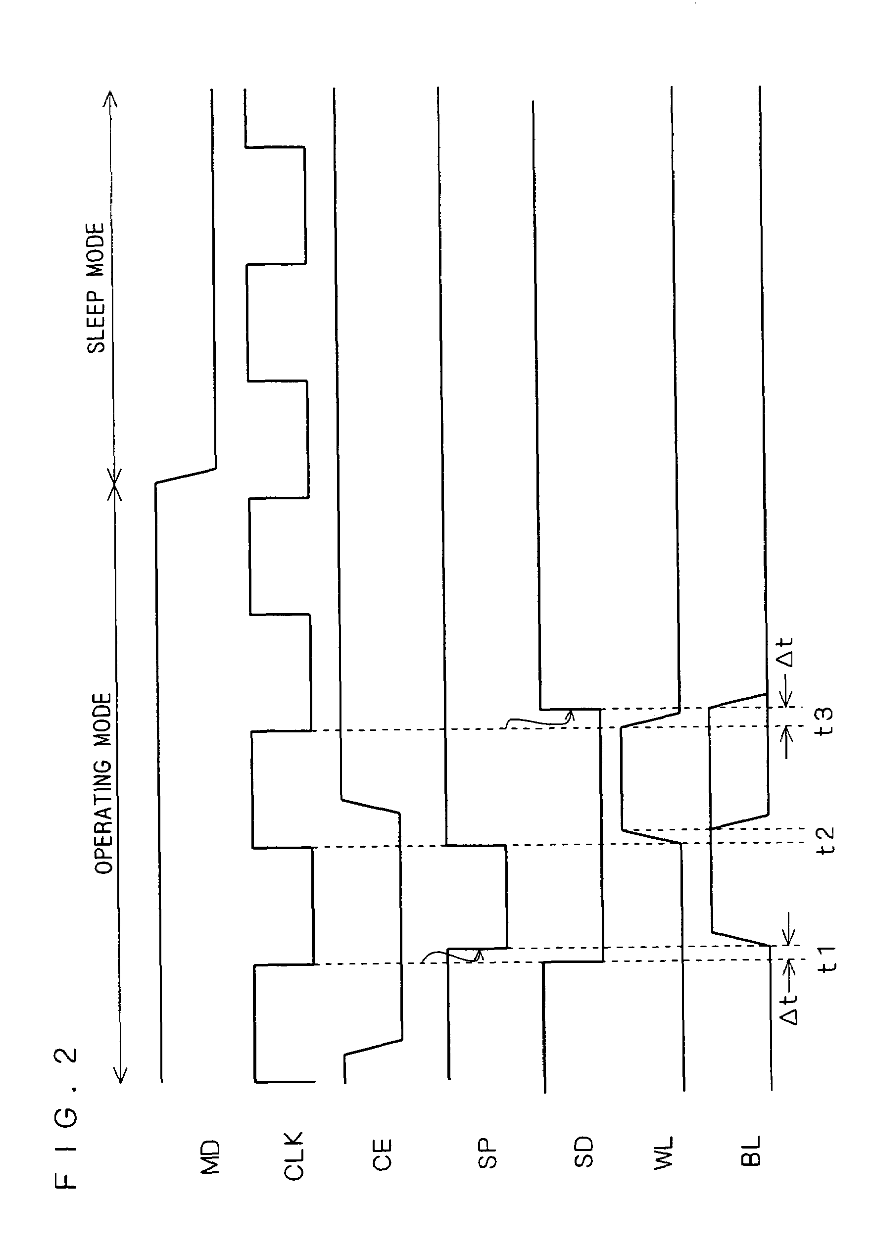
[0045]The data storage circuit of the first preferred embodiment comprises an SRAM cell S1, a precharge circuit for precharging bit lines BL and / BL and a discharge circuit for discharging the bit lines BL and / BL, and the precharge circuit and the discharge circuit are controlled on the basis of a mode signal MD having an operating mode and a sleep mode and a chip enable signal CE.

[0046]Though the data storage circuit comprises a plurality of SRAM cells S1 arranged in a matrix and a plurality of word lines WL used for selecting the respective SRAM cells S1 and a plurality of bit lines BL and / BL, FIG. 1 shows only one SRAM cell S1 and its relevant peripheral circuit in close-up.

[0047]Specific discussion will be made below on...


PUM


Abstract

A data storage circuit having a plurality of memory cells (S1), a plurality of bit lines (BL, / BL) and a precharge circuit further comprises a discharge circuit. In an operating mode of the data storage circuit, the bit lines (BL, / BL) are precharged by the precharge circuit under the control on the basis of a chip enable signal (CE) before write or read of data into / from the memory cells (S1) and in a standby state, the bit lines (BL, / BL) are discharged by the discharge circuit. Further, also in a sleep mode, the bit lines (BL, / BL) are discharged by the discharge circuit. With this circuit configuration and operation, it is possible to provide the data storage circuit which allows reduction in standby power consumption by suppressing standby currents in the standby state.

Description

BACKGROUND OF THE INVENTION[0001]1. Field of the Invention[0002]The present invention relates to a data storage circuit, and more particularly to potential setting of bit lines or match lines.[0003]2. Description of the Background Art[0004]In a static random access memory (SRAM) of the background art, when data is written into the SRAM or read out from the SRAM, bit lines are first precharged.[0005]Usually, precharge of the bit lines is performed during a period while a clock signal indicates “0” level and write or read of data is performed during a period while the clock signal indicates “1” level (see Japanese Patent Application Laid-Open No. 2001-344979, Paragraph No. 0063, FIG. 1 and the like).[0006]Recently, however, with thinning of gate oxide films in size reduction of devices, in the background-art technique where the precharge of the bit lines is performed in a standby state of the SRAM (during the period while no access is made to the SRAM), a gate leak current flowing in ...

Claims


Application Information

Patent Timeline
IPC IPC(8): G11C7/00G06F12/00G11C11/412G11C11/41
CPCG11C11/412
Inventor NOTANI, HIROMI
Owner RENESAS ELECTRONICS CORP
Features
  • R&D
  • Intellectual Property
  • Life Sciences
  • Materials
  • Tech Scout
  • Unparalleled Data Quality
  • Higher Quality Content
  • 60% Fewer Hallucinations
Learn More