Planar avalanche photodiode

a photodiode and avalanche technology, applied in the field of photodetectors, can solve the problems of reducing yield, difficult to passivate using a layer of insulating material, and reducing bandwidth

Inactive Publication Date: 2008-03-25
MACOM TECH SOLUTIONS HLDG INC
View PDF28 Cites 42 Cited by
  • Summary
  • Abstract
  • Description
  • Claims
  • Application Information

AI Technical Summary

Benefits of technology

[0051]As described, various implementations of the present invention provide numerous advantages, for example, the structure of the planar avalanche region. Moreover, the structure of the planar avalanche photodiode 10 and 110 shown in FIGS. 1 and 2, respectively, or 210 and 310 shown in FIGS. 9 and 10, respectively, is reversed from a typical InP / InGaAs avalanche photodiode geometry since electrons are being avalanched in the n-type semiconductor multiplication layer 24 as opposed to the avalanching of holes in an InP multiplication region, as found in conventional avalanche photodiodes. This structural inversion allows the low field region in the InGaAs absorption region to be at the top of the device rather than the high field avalanche region as in a standard InP avalanche photodiode.

Problems solved by technology

A particular type of avalanche photodiode know as a mesa avalanche photodiode exposes high field p-n junctions and large numbers of exposed surface and interface states that make it difficult to passivate using a layer of insulating material.
This combination of guard rings and critically controlled diffusions increases the capacitance, lowers the bandwidth, and reduces the yield, thus increasing the cost of these APDs.
However, a diffused structure is even more difficult to achieve in InAlAs since the larger electron avalanche coefficient (relative to the holes) makes it desirable to multiply the electrons rather than the holes as in standard InP based APDS.
Moreover, simply reversing the standard p-doped diffused structure is not sufficient, since n-dopants do not diffuse fast enough.

Method used


Image

  • Planar avalanche photodiode
  • Planar avalanche photodiode
  • Planar avalanche photodiode

Examples


Embodiment Construction

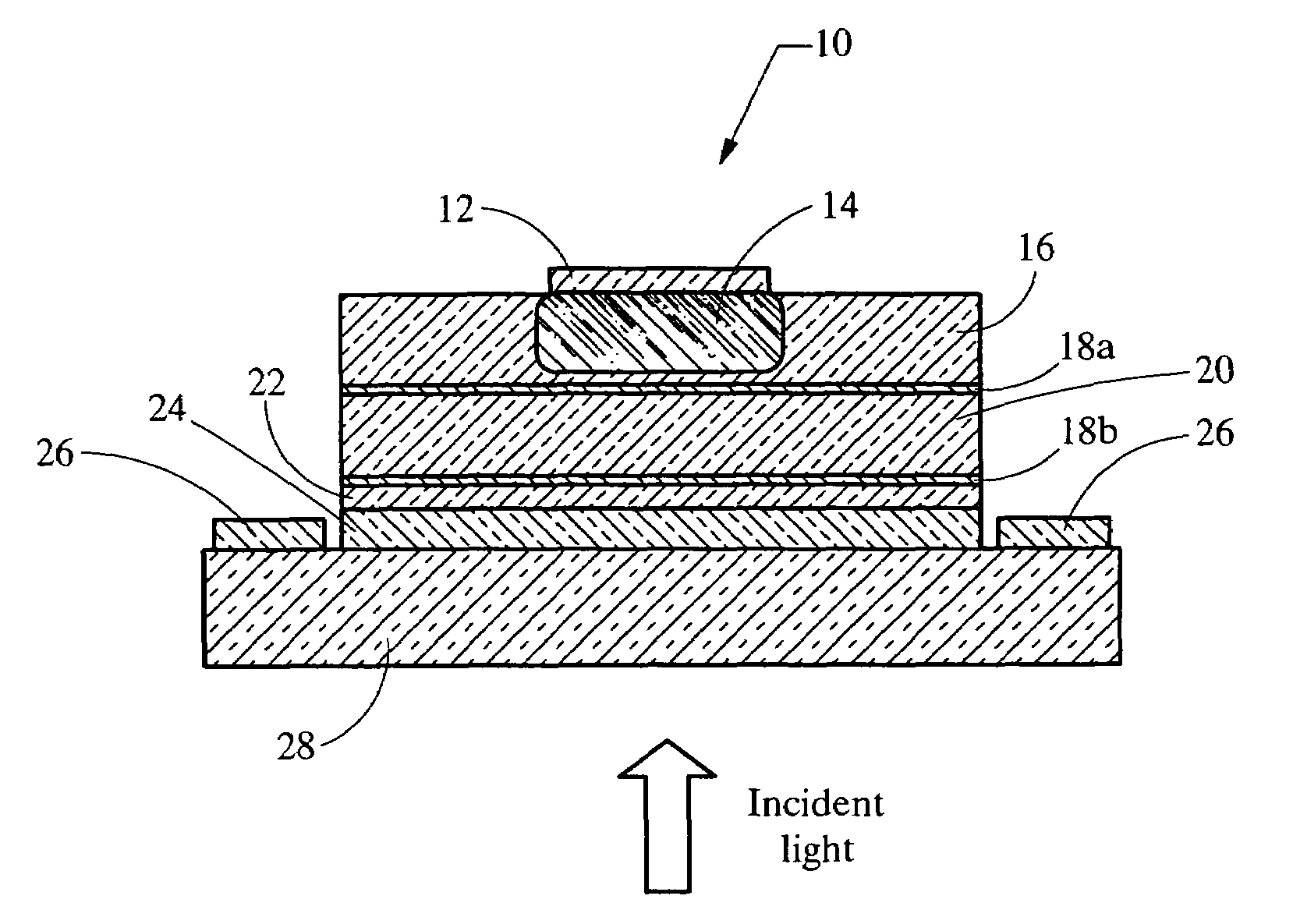
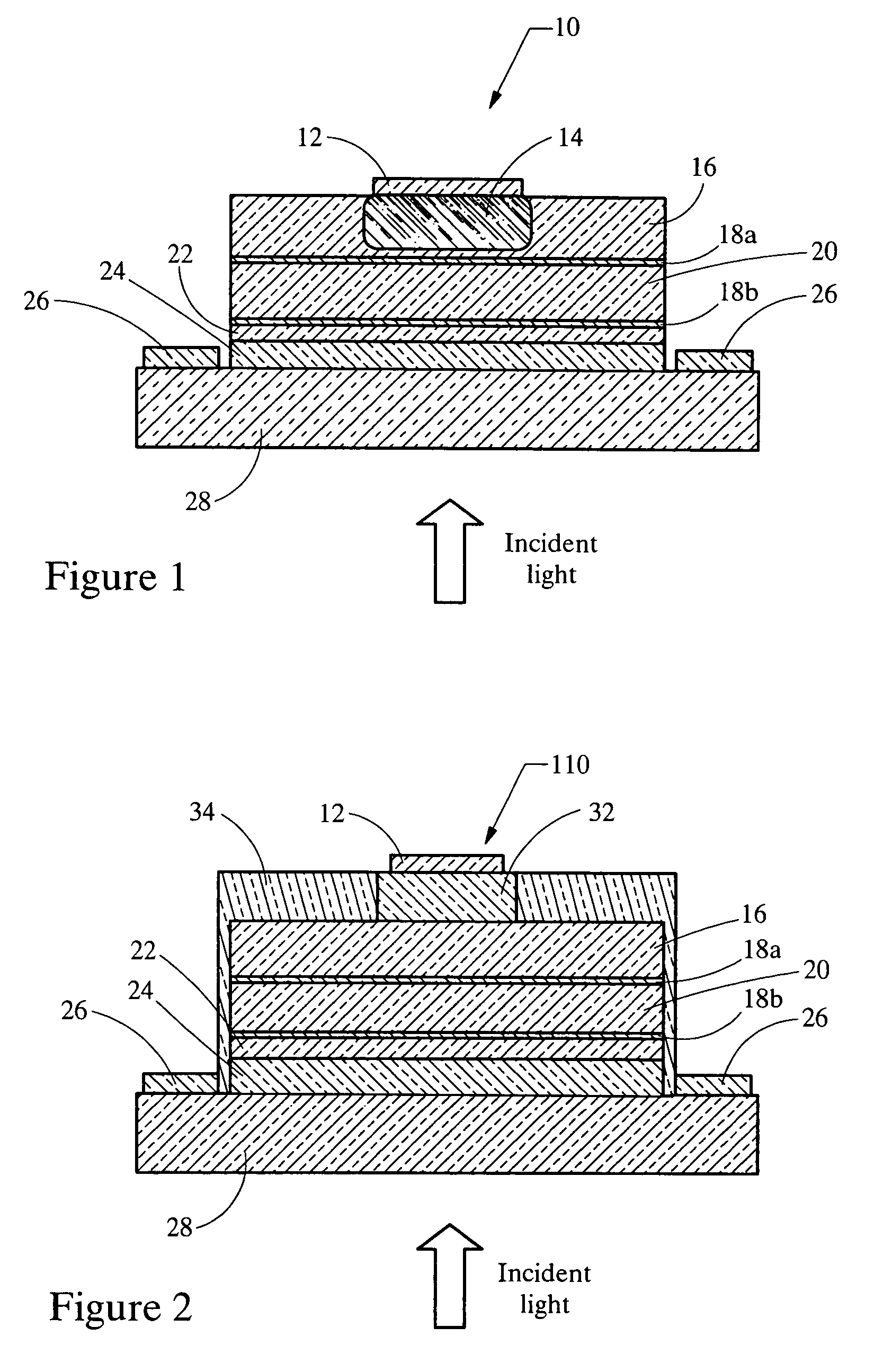
[0024]Referring now to FIG. 1, a photodetector structure, in particular, a planar avalanche photodiode (“APD”), embodying the principles of the present invention is illustrated and designated at 10. As its primary components, the APD 10 includes a p-type contact layer 12 and a first n-type semiconductor layer 28 that defines a second n-type contact layer. The avalanche photodiode 10 is optimized for increased performance through diffused p-type doping creating a p-n junction and a p-contact. Specifically, the p-type contact layer 12 is positioned on a second n-type semiconductor layer 16, which includes a p-type diffusion region 14 to form a p-n junction and create a p-contact to the second n-type semiconductor layer 16. Alternatively, the semiconductor layer 16 can be a p type so that a p-p+ junction is formed by the diffusion. The semiconductor layer 16 can be undoped or low doped to facilitate forming a depletion region under a bias voltage.

[0025]The planar avalanche photodiode 1...


PUM


Abstract

A planar avalanche photodiode includes a small localized contact layer on the top of the device produced by either a diffusion or etching process and a semiconductor layer defining a lower contact area. A semiconductor multiplication layer is positioned between the two contact areas and a semiconductor absorption layer is positioned between the multiplication layer and the upper contact layer. The photodiode has a low capacitance and a low field near the edges of the semiconductor multiplication and absorption layers.

Description

RELATED APPLICATIONS[0001]This application is a continuation-in-part of International PCT Application No. US03 / 03323, filed Feb. 3, 2003, which claims the benefit of U.S. Provisional Application Nos. 60 / 353,530 and 60 / 353,765, both of which were filed Feb. 1, 2002.[0002]The entire contents of the above applications are incorporated herein by reference.BACKGROUND[0003]The present invention relates to photodetectors. More specifically, the present invention relates to avalanche photodiodes.[0004]Owing to the known interaction between photons and electrons, advances have been made in the field of photodetectors in recent years, particularly in those photodetectors that utilize semiconductor materials. One type of semiconductor-based photodetector known as an avalanche photodiode includes a number of semiconductive materials that serve different purposes such as absorption and multiplication.[0005]The avalanche photodiode structure provides a large gain through the action of excited cha...

Claims


Application Information

Patent Timeline
Patent Type & Authority Patents(United States)
IPC IPC(8): H01L29/732H01LH01L21/00H01L31/0328H01L31/072H01L31/107H01L31/109
CPCH01L31/107H01L31/1075H01L31/035281Y02E10/50
Inventor KO, CHENG C.LEVINE, BARRY
Owner MACOM TECH SOLUTIONS HLDG INC
Why Eureka
Try Eureka