Solid-state color imaging apparatus capable of reducing false signals with regard to both luminance and chrominance

a color imaging and solid-state technology, applied in the field of solid-state color imaging apparatus, can solve the problems of large number, camera without a change in frame rate, and inability to output an image signal to a display, and achieve the effects of reducing the aliasing of a high-frequency component appearing as low frequency, enhancing sensitivity, and enhancing the sensitivity

Active Publication Date: 2008-03-25
PANASONIC SEMICON SOLUTIONS CO LTD
View PDF15 Cites 29 Cited by
  • Summary
  • Abstract
  • Description
  • Claims
  • Application Information

AI Technical Summary

Benefits of technology

[0008]It is therefore an object of the present invention to reduce the number of pixels output from a solid-state imaging device having a large number of pixels such as an ultra megapixel solid-state imaging device by utilizing a pixel adding technique for taking pictures at high speed with low power consumption, high sensitivity and high image quality (i.e., with high-frequency aliasing noise suppressed), thus allowing an ultra megapixel solid-state imaging device to pickup moving images.
[0012]All the pixels in an effective area of the solid-state imaging device may be targets of pixel additions. Then, all the pixels can be output by the pixel additions without being discarded, thus greatly enhancing the sensitivity. According to the present invention, the percentage of utilized pixels is 100%.
[0013]Basic units of the pixel adding area may be arranged to overlap with each other such that the resultant pixels reduced in number and obtained by the addition are regularly arranged. Then, even if an image whose video signal includes high-frequency signals in both the horizontal and vertical directions is captured, aliasing of a high-frequency component appearing as low frequencies is greatly reduced and false signals in both of luminance signals and chrominance signals are largely suppressed and, in addition, the image sampling densities in the horizontal and vertical directions are perfectly balanced. Accordingly, it is possible to set the horizontal resolution and the vertical resolution exactly equal to each other.
[0014]The second solid-state color imaging apparatus reduces the number of output pixels in capturing a moving image by an ultra megapixel solid-state imaging device, as compared to the first solid-state color imaging apparatus. As a result, the second solid-state color imaging apparatus has a great effect in reducing the number of pixels to a necessary number while maintaining high image quality.

Problems solved by technology

Therefore, in many cases, the solid-state imaging device cannot output an image signal to a display (e.g., a liquid-crystal monitor) of a camera without a change in frame rate.
This causes not only the problem of a large number of false signals in both of luminance (Y) signals and chrominance (C) signals but also the problem of large decrease in the vertical resolution with respect to the horizontal resolution caused by an imbalance in pixel sampling density between the horizontal direction and the vertical direction.
In addition, since signals of pixels on lines from which no data is read out are discarded, there also arises another problem that substantial sensitivity decreases.
As the number of pixels in a solid-state imaging device increases, all the foregoing problems inherently tend to be more noticeable with the conventional method.
However, with this technique, pixels which are not a target of the pixel addition are present in an effective area in the solid-state imaging device, so that high-sensitivity imaging is not achieved.
In addition, pixels reduced in number for respective colors and obtained by the addition are irregularly arranged, resulting in defects in the image.

Method used


Image

  • Solid-state color imaging apparatus capable of reducing false signals with regard to both luminance and chrominance
  • Solid-state color imaging apparatus capable of reducing false signals with regard to both luminance and chrominance
  • Solid-state color imaging apparatus capable of reducing false signals with regard to both luminance and chrominance

Examples


embodiment 1

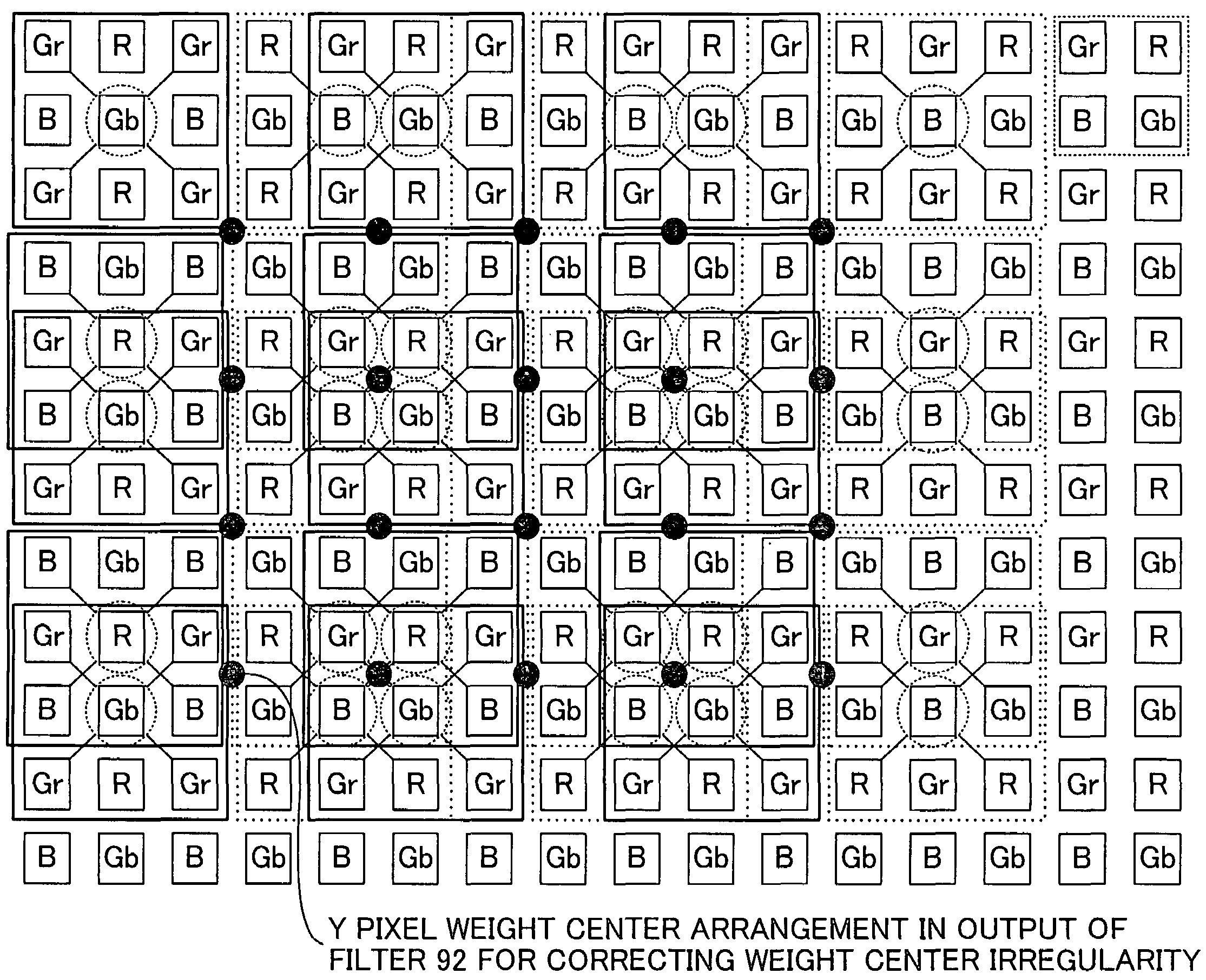
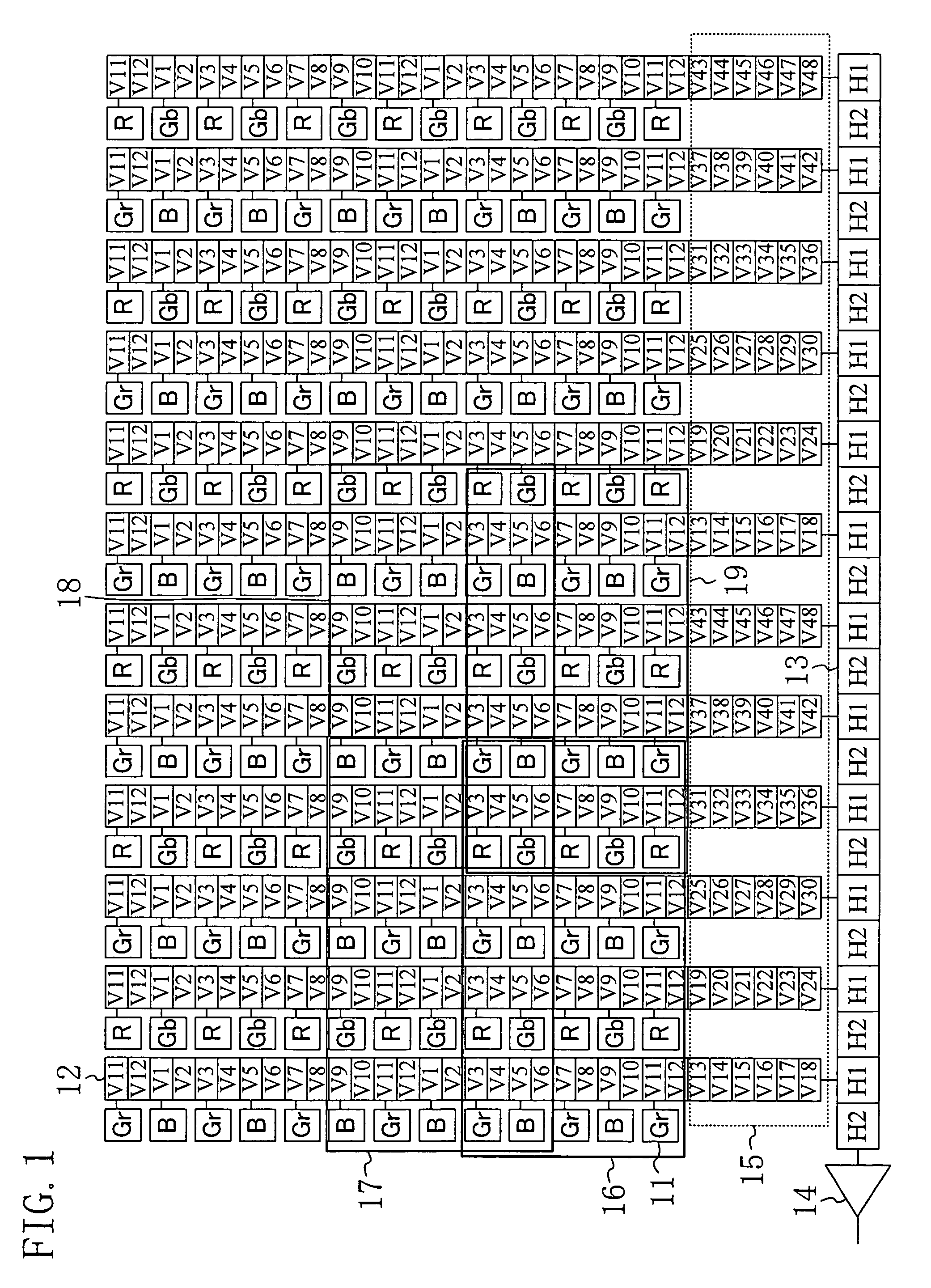
[0031]FIG. 1 is a diagram showing a configuration of a CCD solid-state imaging device according to a first embodiment of the inventive solid-state color imaging apparatus. Reference numeral 11 denotes a photoelectric converter and a color filter attached to the front face thereof. In this embodiment, color filters each for red (R), green (G) or blue (B) are adopted and are arranged in the manner of a Bayer arrangement, for example. Though Gr and Gb are actually the same color (green), filter pixels horizontally sandwiched between R filters are shown as Gr and filter pixels horizontally sandwiched between B filters are shown as Gb for convenience in describing operation. Reference numeral 12 denotes a vertical transfer stage in 12 phases constituted by V1 through V12. Reference numeral 13 denotes a horizontal transfer stage in two phases constituted by H1 and H2. Reference numeral 14 denotes an output amplifier. Reference numeral 15 denotes a vertical-horizontal transfer control sect...

embodiment 2

[0042]FIG. 5 is a diagram showing a configuration of a CCD solid-state imaging device according to a second embodiment of the inventive solid-state color imaging apparatus. Reference numeral 51 denotes a photoelectric converter and a color filter attached to the front face thereof. In this embodiment, color filters are arranged as a complementary mosaic filter array in two rows and four columns, for example. Reference numeral 52 denotes a vertical transfer stage in 12 phases constituted by V1 through V12. Reference numeral 53 denotes a horizontal transfer stage in three phases constituted by H1 through H3. Reference numeral 54 denotes an output amplifier. Reference numeral 55 denotes a vertical-horizontal transfer control section which is an extension of the 12-phase vertical transfer stage 52 constituted by V1 through V12, has its gates independently wired, and is constituted by V13 through V48. Reference numeral 56 denotes a basic unit of a pixel adding area for Mg. Reference nume...

embodiment 3

[0054]FIG. 7 is a diagram showing a configuration of a CCD solid-state imaging device according to a third embodiment of the inventive solid-state color imaging apparatus. Reference numeral 71 denotes a photoelectric converter and a color filter attached to the front face thereof. In this embodiment, color filters are arranged in the manner of a Bayer arrangement, for example. Reference numeral 72 denotes a vertical transfer stage in eight phases constituted by V1 through V8. Reference numeral 73 denotes a horizontal transfer stage in two phases constituted by H1 and H2. Reference numeral 74 denotes an output amplifier. Reference numeral 75 denotes a vertical-horizontal transfer control section which is an extension of the eight-phase vertical transfer stage 72 constituted by V1 through V8, has its gates independently wired, and is constituted by V9 through V24. Reference numeral 76 denotes a basic unit of a pixel adding area for Gr. Reference numeral 77 denotes a basic unit of a pi...


PUM


Abstract

A pixel area of a megapixel solid-state color imaging device is divided into unit areas for pixel adding and all the pixels for the same color are added together in each unit area. Accordingly, the percentage of utilized pixels is raised to 100% and aliasing noise to low frequencies in a high-frequency video signal is greatly suppressed by a spatial LPF (low pass filter) effect of the pixel addition in the area units.

Description

BACKGROUND OF THE INVENTION[0001]The present invention relates to solid-state color imaging apparatus such as a digital still camera or a digital video camera.[0002]Solid-state imaging devices for converting incident light into an electric signal and outputting the signal as an image signal have been previously known, and cameras such as a digital still camera for displaying the image signal obtained by such a solid-state imaging device as a still image have been also known. In recent years, cameras using such solid-state imaging devices have been required to have their image qualities and functions further improved, and the number of pixels used therein has been increased rapidly.[0003]In a solid-state imaging device having about 5 million pixels, for example, about 1920 pixels are provided in the vertical direction and about 2560 pixels are provided in the horizontal direction. The number of pixels of this device is about 16 times as large as that of a general NTSC (national telev...

Claims


Application Information

Patent Timeline
Patent Type & Authority Patents(United States)
IPC IPC(8): H04N3/14H04N5/335H01L27/148H01L27/146H01L31/10H04N5/341H04N5/367H04N5/369H04N5/3722H04N5/378H04N9/04H04N9/07
CPCH04N3/1562H04N9/045H04N5/23245H04N23/667H04N25/46H04N25/73H04N25/136H04N25/134F25D31/002B67D2001/0093F25D2400/38
Inventor FUJII, TOSHIYAIWASAWA, TAKAHIROYAMAGUCHI, TAKUMIMURATA, TAKAHIKO
Owner PANASONIC SEMICON SOLUTIONS CO LTD
Why Eureka
Try Eureka