[0014]One
advantage of the invention is that the venting element thermally insulates at least a first portion of the body structure from at least a second portion of the body structure, which reduces
thermal coupling between the first and second portions. In certain embodiments the venting element is disposed in the body structure and produces a stagnant vapor region that reduces convective transport between venting element surfaces. As described above, the body structure optionally includes the venting element disposed at least partially therethrough (e.g., completely through the body structure). In these embodiments, the method optionally further includes bonding at least one additional substrate over at least a segment of the venting element to produce a stagnant vapor region that reduces convective transport between venting element surfaces. In preferred embodiments, at least one of the first and second portions further includes at least one cavity disposed therein. Optionally, the at least one cavity includes a plurality of cavities in which at least two adjacent cavities include one or more venting elements disposed therebetween.
[0015]As mentioned, although the methods of the invention are applicable to a wide array of manufacturing processes, in preferred embodiments the body structure comprises at least one microfluidic device. In these embodiments, the at least one of the first and second substrates typically also includes at least one cavity, or a portion thereof, disposed thereon. The methods also generally include fabricating one or more ports through at least one of the first or second substrates such that at least one of the one or more ports fluidly communicates with the at least one cavity. Optionally, the methods include fabricating one or more ports through at least one of the first or second substrates such that at least one of the one or more ports fluidly communicates with the at least one venting element (i.e., not in fluid communication the at least one cavity), e.g., to vent bond voids from the at least one venting element through the one or more ports during substrate bonding.
[0016]The methods optionally include fabricating the at least one venting element to include at least one venting
channel network, a plurality of venting cavities, or both. Optionally, the methods include fabricating each of the plurality of venting cavities to include regularly or irregularly shaped cavities, each cavity including three dimensions, in which two of the three dimensions together form a shape that includes a triangle, a square, a rectangle, a trapezoid, a regular n-sided polygon, an irregular nsided polygon, a circle, an oval, or the like. Each of the plurality of venting cavities is optionally fabricated at regular or irregular intervals (e.g., at least about 10 μm) from one another.
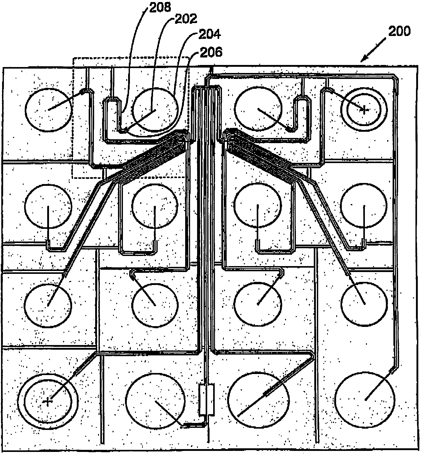
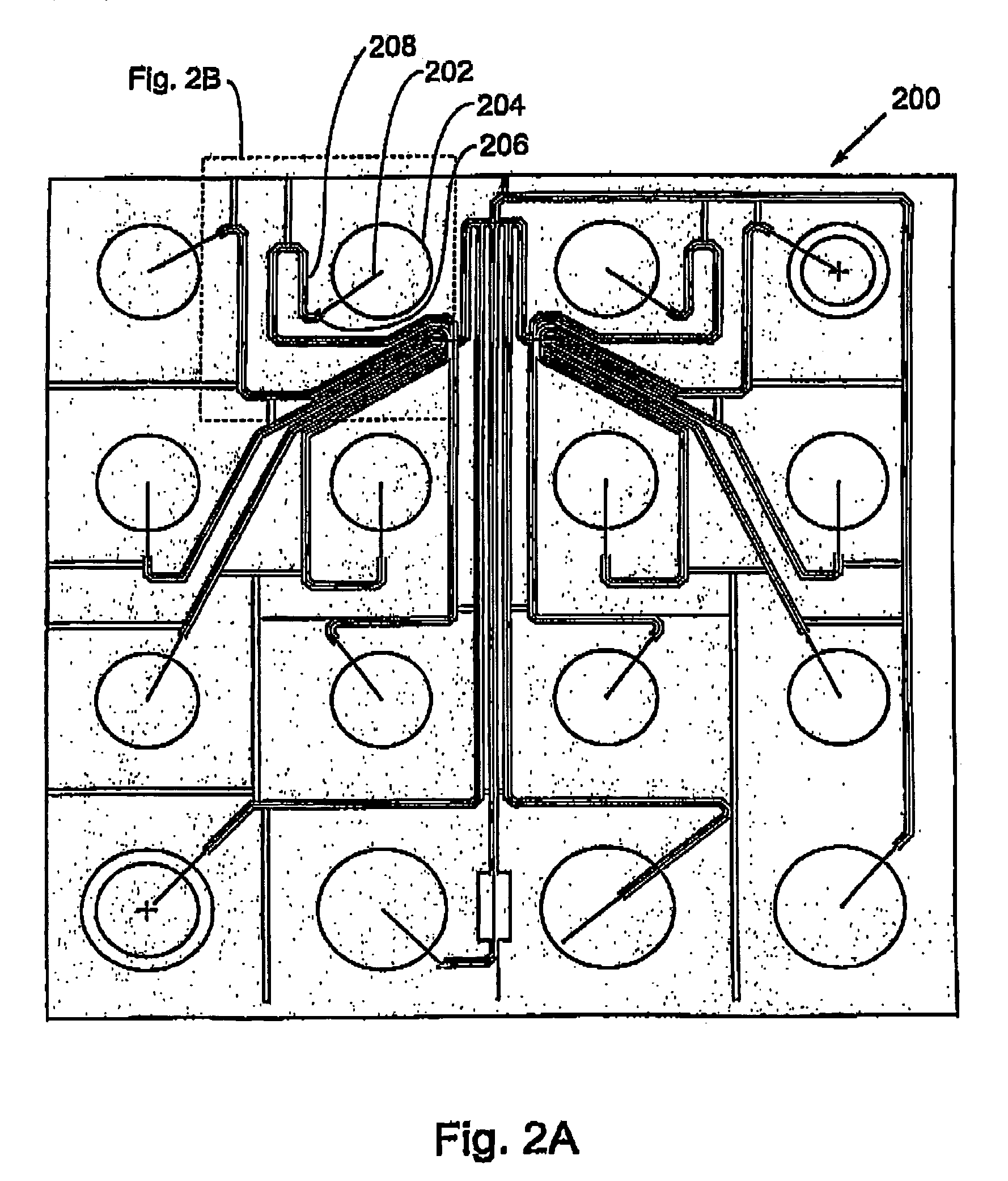
[0017]In embodiments where the body structure is a microfluidic device, the methods generally include fabricating the at least one cavity to include a microchannel network. In these embodiments, the at least one venting
channel network typically includes a first venting
channel network, at least one venting channel of which is disposed proximal to a first side of one or more microchannels in the microchannel network. The methods also optionally include fabricating a second venting channel network, at least one venting channel of which is disposed proximal to a second side of the one or more microchannels in the microchannel network. Typically, the at least one venting channel of the first and second venting channel networks are fabricated to be disposed substantially parallel to the one or more microchannels.
[0018]The methods of the present invention include fabricating the first and second venting channel networks in various alternative configurations. For example, the at least one venting channel of the first and second venting channel networks are typically fabricated to terminate at least about 0.05 mm (e.g., 0.1 mm, 0.3 mm, 0.5, mm, 1 mm, or more) from an edge of a port when the one or more microchannels fluidly communicate with the port. The methods also include fabricating the at least one venting channel of the first and second venting channel networks to each comprise a width of at least about 5 μm (e.g., 10 μm, 50 μm, 100 μm, or more). Optionally, the at least one venting channel of the first and second venting channel networks are fabricated to each include cross-sectional midpoints disposed at least about 60 μm from a cross-sectional midpoint of the one or more microchannels. The one or more microchannels are typically fabricated to include a width of at least about 60 μm. Furthermore, the methods optionally include merging two or more venting channels in the first or second venting channel networks in regions where cross-sectional midpoints of two or more venting channels are separated by less than about 50 μm.
[0019]In certain embodiments, the methods of the invention include fabricating a third venting channel network that includes one or more venting channels proximal to one or more edges of the body structure. The one or more venting channels typically include widths of at least about 0.1 mm. Additionally, the methods optionally include fabricating the one or more venting channels at least about 3 mm from the one or more edges of the body structure. In these embodiments, the one or more venting channels of the first and second venting channel networks are typically fabricated to be in fluid communication with the third venting channel network.

