Isothermal co-emitter lateral sige heterojunction bipolar transistor
A heterojunction bipolar, co-emission technology, used in semiconductor devices, electrical solid devices, electrical components, etc., can solve the problems of uneven temperature distribution of devices, aggravate device thermal problems, device performance degradation, etc. Stable work, improved heat dissipation, reduced thermal resistance
- Summary
- Abstract
- Description
- Claims
- Application Information
AI Technical Summary
Problems solved by technology
Method used
Image
Examples
Embodiment 1
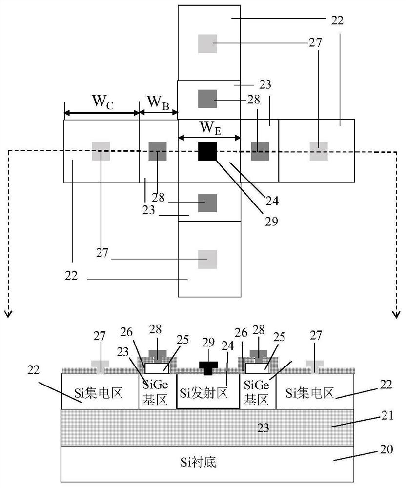
[0034] figure 2 Illustrated top and cross-sectional structural schematic diagrams of a common-emitter lateral SiGe HBT with four sub-transistors, including Si substrate (20), SiO 2 Buried oxide layer (21), and located in SiO 2 Si collector region (22), SiGe base region (23), Si emitter region (24) above the buried oxide layer (21); the SiO 2 The buried oxide layer (21) is located directly above the Si substrate (20), and has a thickness of 20 nm; the Si collector region (22) is symmetrically distributed in the center, and the collector region width (W) corresponding to each sub-transistor C ) is 65nm; the width of the emitter region corresponding to each sub-transistor of the Si emitter region (24) (W E ) is 50 nm; the SiGe base region (23) is adjacent to the Si collector region (22) and the Si emitter region (24) and is centrally symmetrically distributed with the Si emitter region (24) as the center of symmetry. Base width (W B ) is 22nm. At the same time, the thicknes...
Embodiment 2
[0037] Figure 4 Illustrated top and cross-sectional structural schematic diagrams of an isothermal co-emitter lateral SiGe HBT with six sub-transistors, including a Si substrate (40), SiO 2 Buried oxide layer (41), and located in SiO 2 Si collector region (42), SiGe base region (43) and Si emitter region (44) directly above the buried oxide layer (41); the SiO 2The buried oxide layer (41) is located directly above the Si substrate (40), and has a thickness of 20 nm; the Si collector region (42) is symmetrically distributed in the center, and the width of the collector region corresponding to each sub-transistor (W C ) is 65nm; the width of the emitter region corresponding to each sub-transistor of the Si emitter region (44) (W E ) is 86.6 nm; the SiGe base region (43) is adjacent to the Si collector region (42) and the Si emitter region (44) and is centrally symmetric with the Si emitter region (44) as the center of symmetry, and each sub-transistor corresponds to The base...
PUM
| Property | Measurement | Unit |
|---|---|---|
| thickness | aaaaa | aaaaa |
| width | aaaaa | aaaaa |
| thickness | aaaaa | aaaaa |
Abstract
Description
Claims
Application Information


