Solid-state radiation detector
- Summary
- Abstract
- Description
- Claims
- Application Information
AI Technical Summary
Problems solved by technology
Method used
Image

Examples
Embodiment Construction
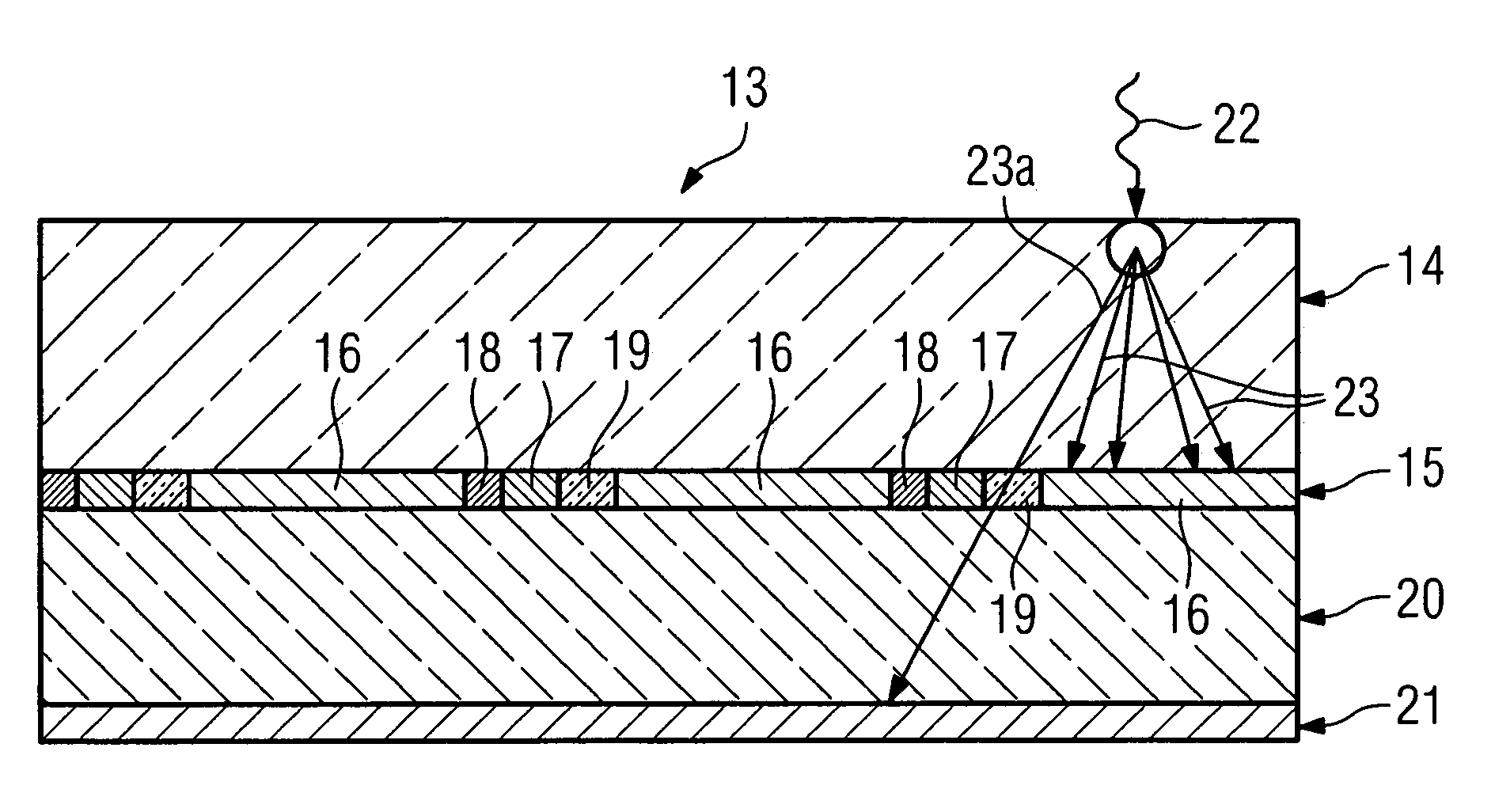
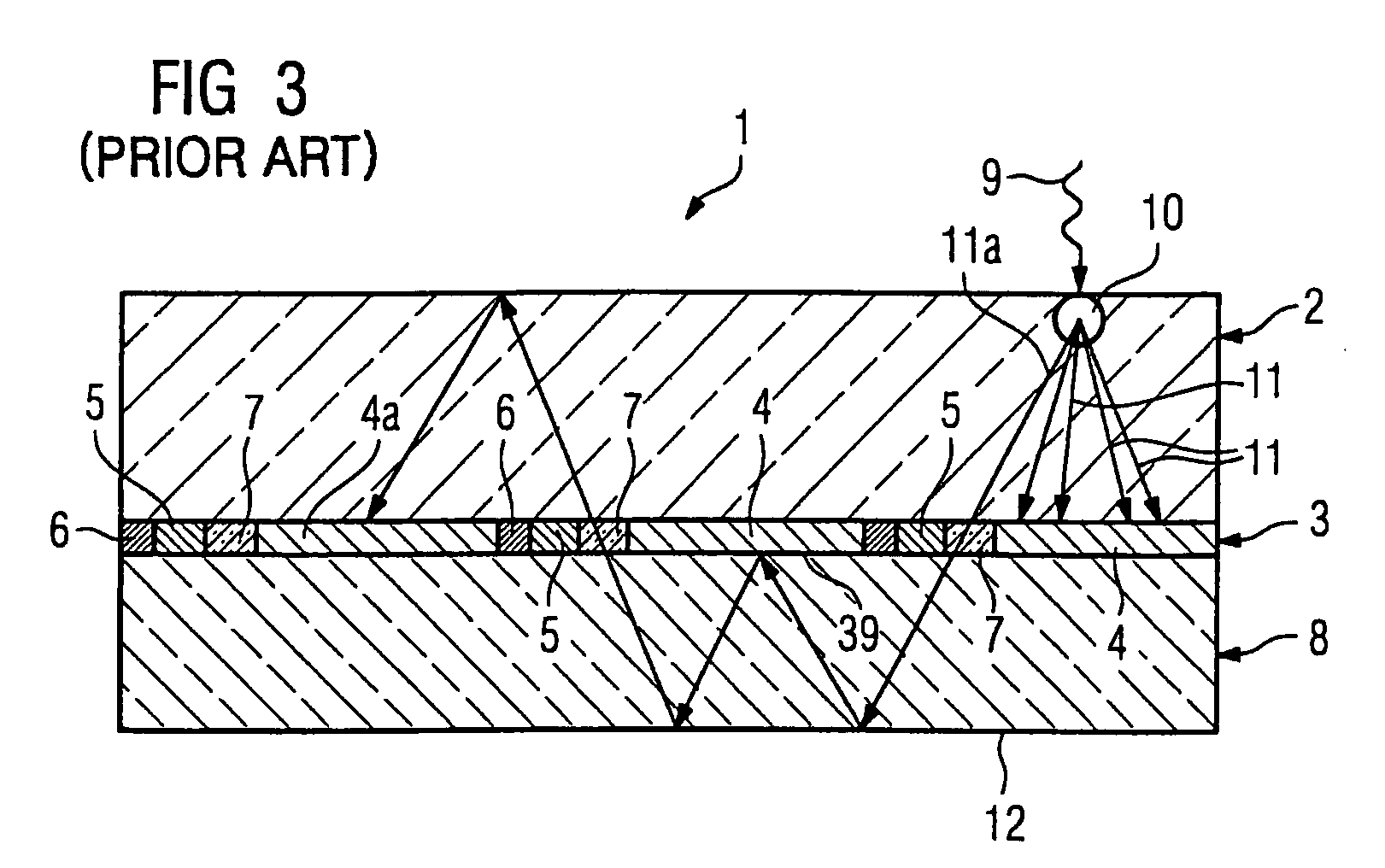
[0024]FIG. 3 shows a solid-state radiation detector 1 in accordance with the prior art. This detector has a scintillator layer 2, for example including a multiplicity of CsI needles grown in parallel on a carrier (not shown in greater detail). Said scintillator layer 2 is coupled to a pixel matrix 3, for example made of amorphous silicon or crystalline silicon. The pixel matrix 3 includes a multiplicity of individual photodiodes 4 with assigned TFT switches 5 and corresponding data lines 6. Situated between the individual photodiodes are transparent regions 7 by means of which the photodiodes are insulated from one another. The pixel matrix 3 is arranged on a carrier 8, here a glass substrate.
[0025]If an X-ray quantum 9 enters into the scintillator layer 2, it is converted into individual light quanta 11 at the absorption location 10. Most of the light quanta 11 impinge on the assigned photodiode 4. However, a portion of the light quanta, here the light quantum 11a, enters into the ...
PUM
 Abstract
Description
Claims
Application Information
 - R&D Engineer
- R&D Manager
- IP Professional
- Industry Leading Data Capabilities
- Powerful AI technology
- Patent DNA Extraction
Browse by: Latest US Patents, China's latest patents, Technical Efficacy Thesaurus, Application Domain, Technology Topic.
© 2024 PatSnap. All rights reserved.Legal|Privacy policy|Modern Slavery Act Transparency Statement|Sitemap