
Multispectral detector matrix

a detector matrix and multi-spectral technology, applied in the field of matrix of multi-spectral detectors, can solve the problems of loss of the compactness of the detector matrix, the disadvantage of rapidly recombining the photo-generated electron-hole pairs, and the loss of around two thirds of light intensity by absorption in the filter

Inactive Publication Date: 2008-04-01
COMMISSARIAT A LENERGIE ATOMIQUE ET AUX ENERGIES ALTERNATIVES
View PDF9 Cites 13 Cited by
  • Summary
  • Abstract
  • Description
  • Claims
  • Application Information

AI Technical Summary

Benefits of technology

The patent proposes a new structure for multispectral detectors that overcomes the limitations of previous methods. The structure includes a matrix of layers separated by layers of dielectric material. The dielectric layers absorb light at different wavelengths, creating electrical charges that can be measured. By calculating the intensities of each wavelength range and using complexation techniques, the structure can provide sufficient information to reconstruct the light intensity. The use of dielectric layers allows for the separation of electrical charges created at different depths in the material. The structure can be designed to have the desired sensitivity for each wavelength range and can be used for imaging applications.

Problems solved by technology

Moreover, around two thirds of the light intensity is lost by absorption in the filters.
This solution overcomes the limitations of the previous solution, but the advantages of compactness of a matrix of detectors are lost.
Other solutions, less used, call on other optical components such as networks, but at least one of the disadvantages mentioned in the previous solutions are also found in them.
Said highly doped zones have the disadvantage of rapidly recombining the photo-generated electron-hole pairs.

Method used


Image

  • Multispectral detector matrix
  • Multispectral detector matrix
  • Multispectral detector matrix

Examples


first embodiment

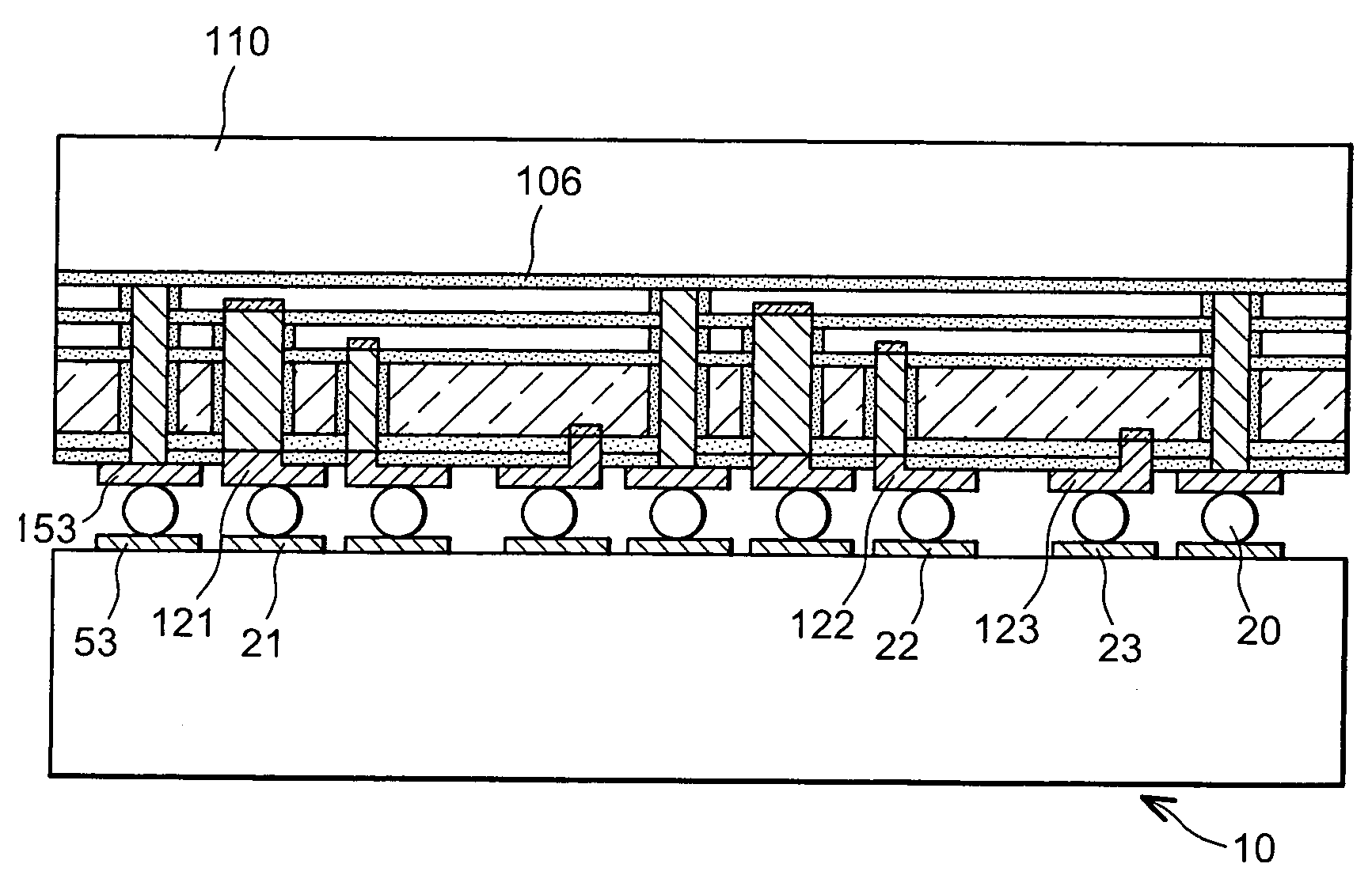
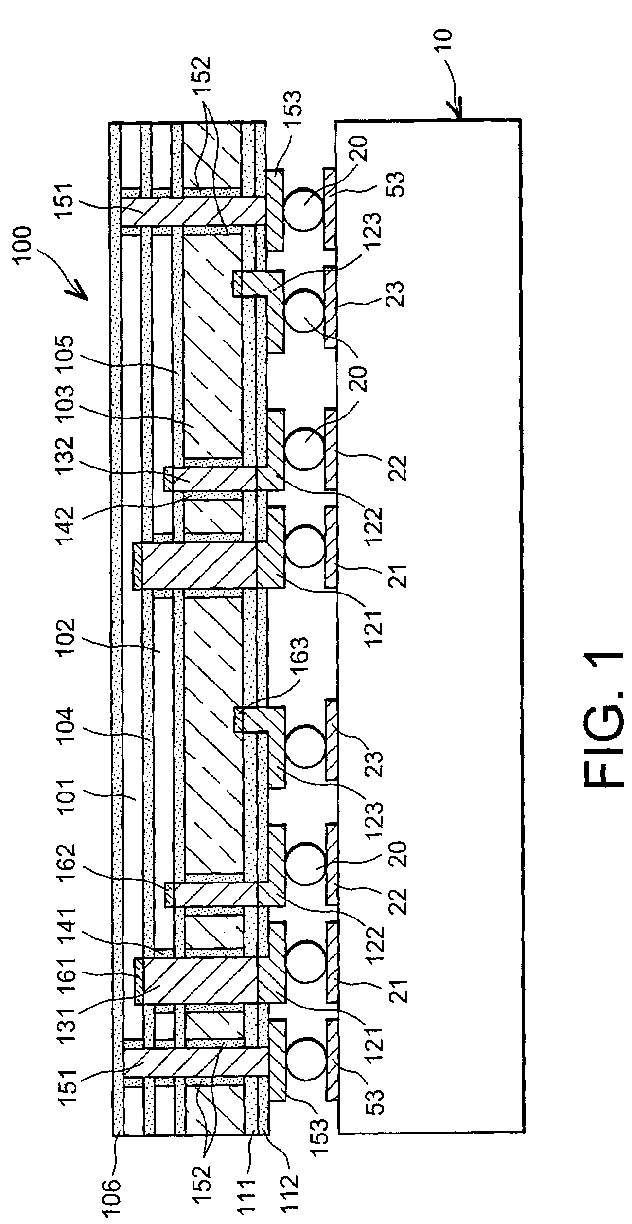
[0024]FIG. 1 is a transversal cross-sectional view of a matrix of multispectral detectors according to the invention, hybridised to a reading circuit;

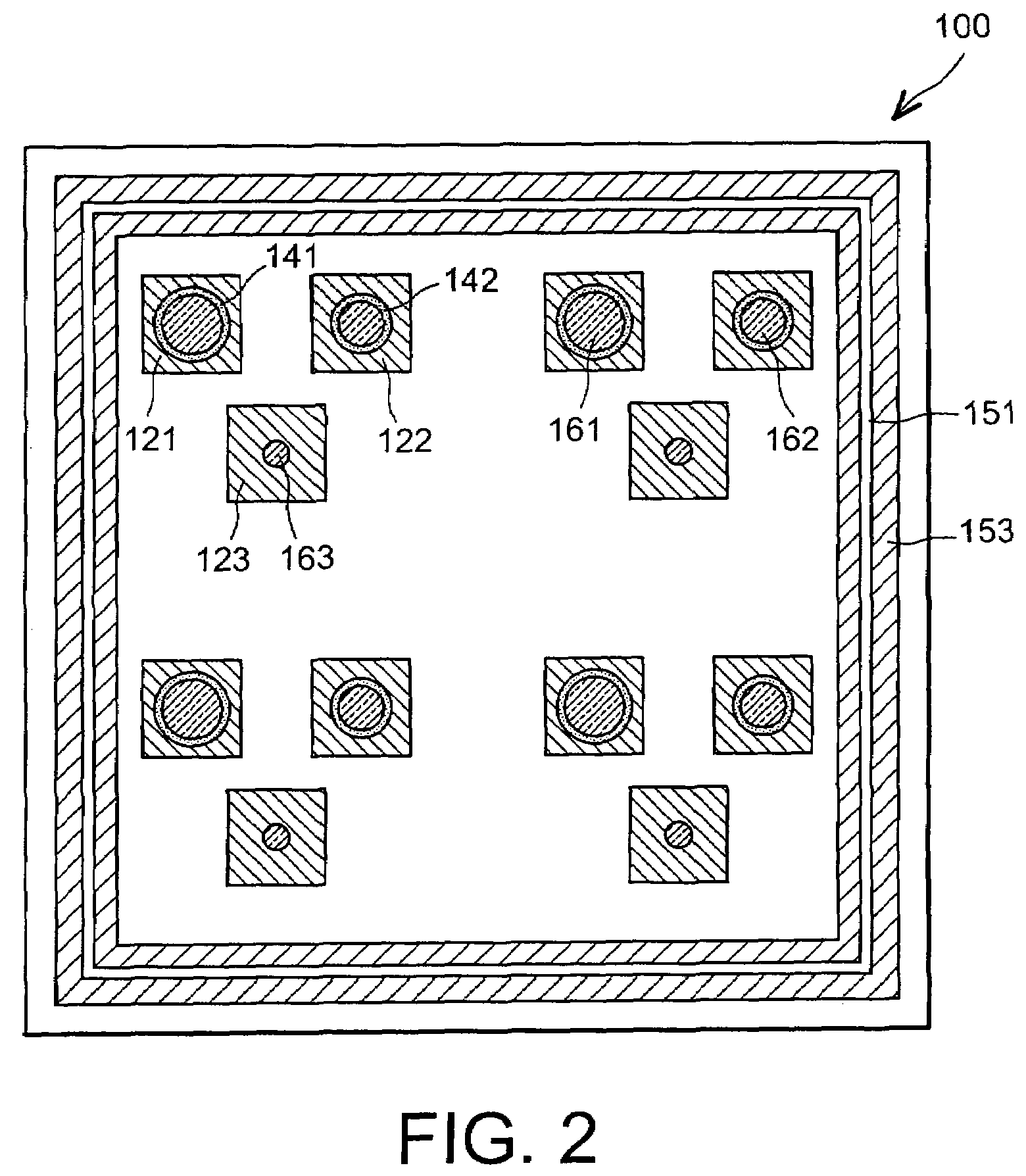
[0025]FIG. 2 is an overhead view of a matrix of multispectral detectors of the type of the first embodiment according to the invention;

second embodiment

[0026]FIG. 3 is a transversal cross-sectional view of a matrix of multispectral detectors according to the invention, hybridised to a reading circuit;

[0027]FIG. 4 is an overhead view of a matrix of multispectral detectors of the type of the second embodiment according to the invention;

third embodiment

[0028]FIG. 5 is an overhead view of a matrix of multispectral detectors according to the invention;

[0029]FIG. 6 is a graph representing light absorption curves in a semiconductor material for three different wavelengths;

[0030]FIGS. 7A to 7R illustrate a method for forming the second embodiment of a matrix of multispectral detectors according to the invention.


PUM


Abstract

The invention concerns a matrix structure of multispectral detectors (200) comprising:a superimposition of several layers of semiconductor material separated by layers of dielectric material transparent to a light to be detected, said superimposition offering a face for receiving the light to be detected, said superimposition of layers of semiconductor material being spread out in picture elements or pixels, each part of the layer of semiconductor material corresponding to a pixel comprising a light detection element delivering electrical charges in response to the light received by said detection element,means for collecting the electrical charges delivered by each light detection element, said collection means being electrically connected to electrical connection means (153) and comprising conductive walls (151).

Description

CROSS-REFERENCE TO RELATED APPLICATION[0001]This application claims priority based on International Patent Application No. PCT / FR2003 / 050186, entitled “Multispectral Detector Matrix” by Pierre Gidon, which claims priority of French Application No. 02 / 16178, filed on Dec. 19, 2002, and which was not published in English.TECHNICAL FIELD[0002]The subject of the present invention is a matrix of multispectral detectors. The aim of this type of matrix is usually to retranscribe images. It may also be used to exploit light signals from measurement devices.[0003]The term “light” may be understood in its wider sense, in other words from the infrared to the ultraviolet. The detectors deliver electrical signals in relation to the light intensities received. Each spectral range is transformed into different electrical signals. Depending on the structure of the detectors, this colour information comes out in parallel or successively. Certain matrices deliver, moreover, several signals in paralle...

Claims


Application Information

Patent Timeline
Patent Type & Authority Patents(United States)
IPC IPC(8): H01L31/09H01L27/146
CPCH01L27/14647H01L27/1465H01L27/14652H01L27/1467
Inventor GIDON, PIERRE
Owner COMMISSARIAT A LENERGIE ATOMIQUE ET AUX ENERGIES ALTERNATIVES
Learn More