CMOS imager with selectively silicided gate

a gate and selective technology, applied in the field of improved semiconductor imaging devices, can solve the problems of high power dissipation of large arrays, ccd imagers also suffer from a number, and are susceptible to radiation damage, so as to improve the speed of transistor gates, prevent blockage of photogates, and more conductive layers

Inactive Publication Date: 2005-08-16
ROUND ROCK RES LLC
View PDF16 Cites 13 Cited by
  • Summary
  • Abstract
  • Description
  • Claims
  • Application Information

AI Technical Summary

Benefits of technology

[0021]The present invention provides an imaging device formed as a CMOS integrated circuit using a standard CMOS process. The invention relates to a method for providing a more conductive layer, such as a silicide or a barrier / metal layer, incorporated into the transistor gates of a CMOS imager to improve the speed of the transistor gates, but selectively removing the silicide or barrier / metal from a photogate to prevent blockage of the photogate.

Problems solved by technology

However, CCD imagers also suffer from a number of disadvantages.
For example, they are susceptible to radiation damage, they exhibit destructive read out over time, they require good light shielding to avoid image smear and they have a high power dissipation for large arrays.
Additionally, while offering high performance, CCD arrays are difficult to integrate with CMOS processing in part due to a different processing technology and to their high capacitances, complicating the integration of on-chip drive and signal processing electronics with the CCD array.
While there has been some attempts to integrate on-chip signal processing with the CCD array, these attempts have not been entirely successful.
CCDs may also suffer from incomplete charge transfer from pixel to pixel during charge transfer which also results in image smear.
In the prior art, the desire to incorporate a silicide over the gate stack to improve speed was hampered by the undesirable effect the silicide layer had on the photogate.
It is for this reason that photogate type devices have not been able to use a silicide gate stack.

Method used


Image

  • CMOS imager with selectively silicided gate
  • CMOS imager with selectively silicided gate
  • CMOS imager with selectively silicided gate

Examples


first embodiment

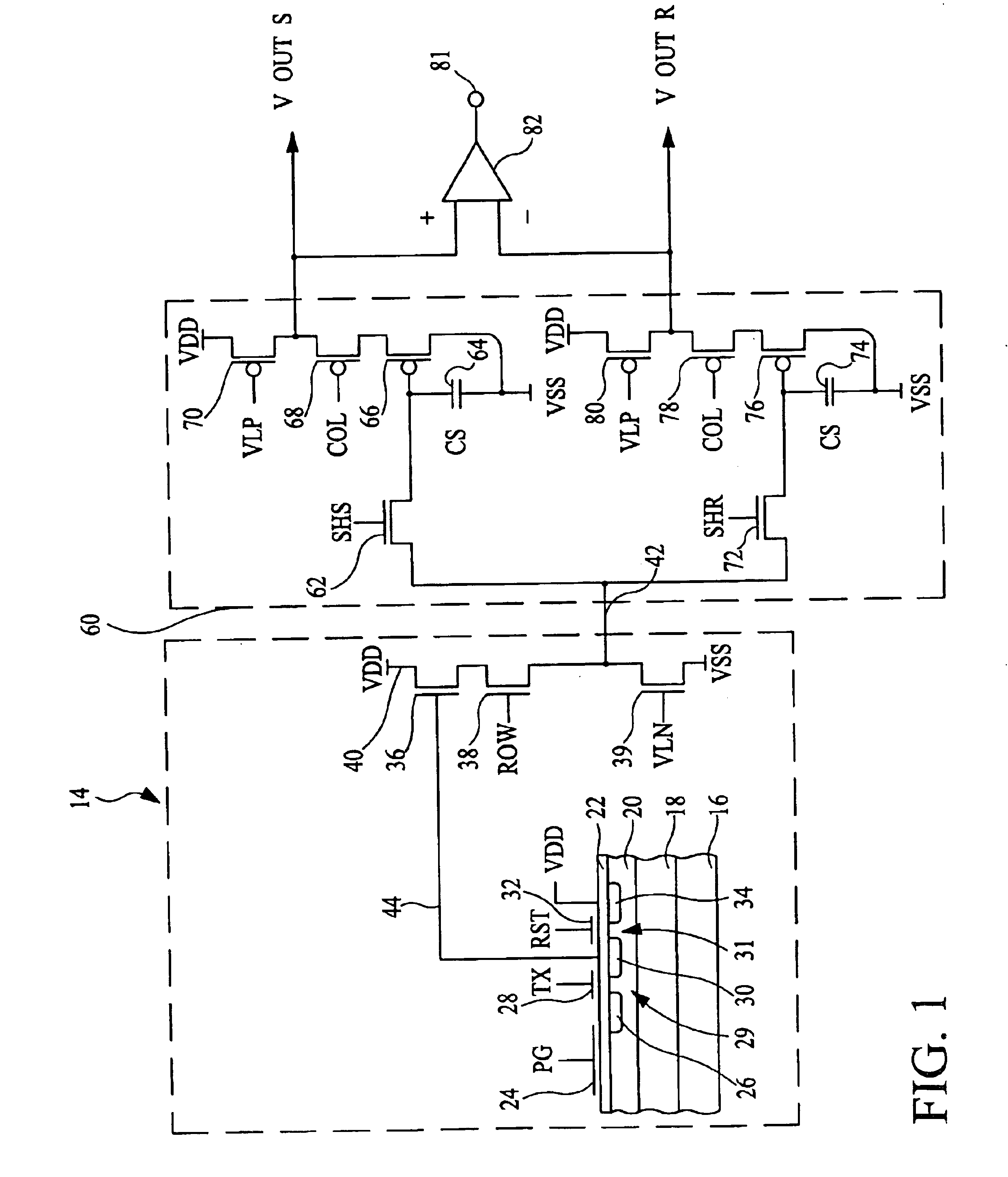
[0049]For the pixel cell of the first embodiment, the photosensor cell is essentially complete at this stage, and conventional processing methods may then be used to form contacts and wiring to connect gate lines and other connections in the pixel cell. For example, the entire surface may then be covered with a passivation layer of, e.g., silicon dioxide, BPSG, PSG, BSG or the like which is CMP planarized and etched to provide contact holes, which are then metallized to provide contacts to the photogate, reset gate, and transfer gate. Conventional multiple layers of conductors and insulators may also be used to interconnect the structures in the manner shown in FIG. 1.

second embodiment

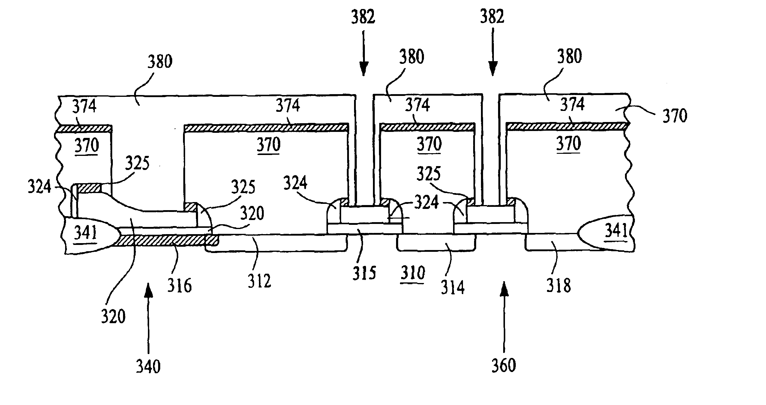
[0050]Reference is now made to FIG. 7. This figure shows a partially cut away side view of a portion of a semiconductor CMOS imager wafer in an interim stage of processing according to the present invention. The imager includes a p-well substrate 310 having n-doped region 316 therein for photocollection. An insulating layer 315 is formed over the substrate 310. The insulating layer is preferably a silicon dioxide grown on the substrate 310 by conventional means such as thermal oxidation of silicon. The substrate 310 has field oxide regions 341 formed to surround and isolate the cells which may be formed by thermal oxidation of silicon using the LOCOS process. While the invention is described with reference to field oxide regions 341, it should be understood that the field oxide regions may be replaced with shallow trench isolation (STI). A doped polysilicon layer 320 may be formed by conventional methods, such as chemical vapor deposition (CVD) over the insulating layer 315. A photo...

third embodiment

[0059]For the pixel cell of the third embodiment, the photosensor cell is essentially complete at this stage, and conventional processing methods may then be used to form contacts and wiring to connect gate lines and other connections in the pixel cell. For example, the entire surface may then be covered with a passivation layer of, e.g., silicon dioxide, BPSG, PSG, BSG or the Like which is CMP planarized and etched to provide contact holes, which are then metallized to provide contacts to the photogate, reset gate, and transfer gate. Conventional multiple layers of conductors and insulators may also be used to interconnect the structures in the manner shown in FIG. 1.

[0060]Reference is now made to FIG. 15. This figure shows a partially cut away side view of a portion of a semiconductor CMOS imager wafer in an interim stage of processing according to a third embodiment of the present invention. The imager includes a substrate 310 preferably doped to a first conductivity type. For ex...


PUM


Abstract

The invention also relates to an apparatus and method for selectively providing a silicide coating over the transistor gates of a CMOS imager to improve the speed of the transistor gates. The method further includes an apparatus and method for forming a self aligned photo shield over the CMOS imager.

Description

[0001]This application is a continuation application of U.S. application Ser. No. 09 / 777,890, filed Feb. 7, 2001, now U.S. Pat. No. 6,611,013, issued Aug. 26, 2003, which is a divisional application of U.S. application Ser. No. 09 / 374,990, filed Aug. 16, 1999, now U.S. Pat. No. 6,333,205, issued Dec. 25, 2001, both of which are incorporated herein by reference in their entirety.FIELD OF THE INVENTION[0002]The invention relates generally to improved semiconductor imaging devices and in particular to an imaging device which can be fabricated using a standard CMOS process. Particularly, the invention relates to a method for providing a silicide coating over the transistor gates used in a CMOS imager to improve the operating speed of the transistors.DISCUSSION OF RELATED ART[0003]There are a number of different types of semiconductor-based imagers, including charge coupled devices (CCDs), photodiode arrays, charge injection devices and hybrid focal plane arrays. CCDs are often employed ...

Claims


Application Information

Patent Timeline
Patent Type & Authority Patents(United States)
IPC IPC(8): H01L27/146H04N5/335
CPCH01L27/14603H01L27/14609H01L27/1462H01L27/14623H01L27/14643H01L27/14687H01L27/14689
Inventor RHODES, HOWARD E.
Owner ROUND ROCK RES LLC
Why Eureka
Try Eureka