Compound semiconductor switching circuit device

a switching circuit and semiconductor technology, applied in the field of compound semiconductor switching circuit devices, can solve the problems of increasing manufacturing costs, small size of logic circuits, and extremely vulnerable to static electricity,

Inactive Publication Date: 2008-04-15
SEMICON COMPONENTS IND LLC
View PDF12 Cites 5 Cited by
  • Summary
  • Abstract
  • Description
  • Claims
  • Application Information

AI Technical Summary

Benefits of technology

[0007]However, an enhancement type FET (hereinafter referred to as an E-FET) that constitutes a logic circuit is small and extremely vulnerable to static electricity. In order to absorb noise and prevent oscillation, a capacitor Ci is connected to an input signal side of the logic circuit, and a capacitor Cr is connected to an inverted signal side thereof. These capacitors Ci and Cr are also vulnerable to static electricity.
[0172]Furthermore, since the conduction regions near the pads can be employed, the protecting element can be formed in the unused spaces between the pads. Therefore, special space for arranging the protecting element is not required, and the size of a chip can be reduced.

Problems solved by technology

However, an enhancement type FET (hereinafter referred to as an E-FET) that constitutes a logic circuit is small and extremely vulnerable to static electricity.
These capacitors Ci and Cr are also vulnerable to static electricity.
Since this process complicates the manufacturing processing, an increase in the manufacturing costs becomes a problem.
In addition, a space for arranging the pn junction diode is also required, so that a size of a chip is increased and there is a further rise in manufacturing costs.
Furthermore, for a microwave device, parasitic capacity will be increased and the characteristic deteriorated due to a connection of the protecting diode.
That is, in a case involving the logic circuit of the switching MMIC, there has been a problem that a switching speed will be reduced.

Method used


Image

  • Compound semiconductor switching circuit device
  • Compound semiconductor switching circuit device
  • Compound semiconductor switching circuit device

Examples


first embodiment

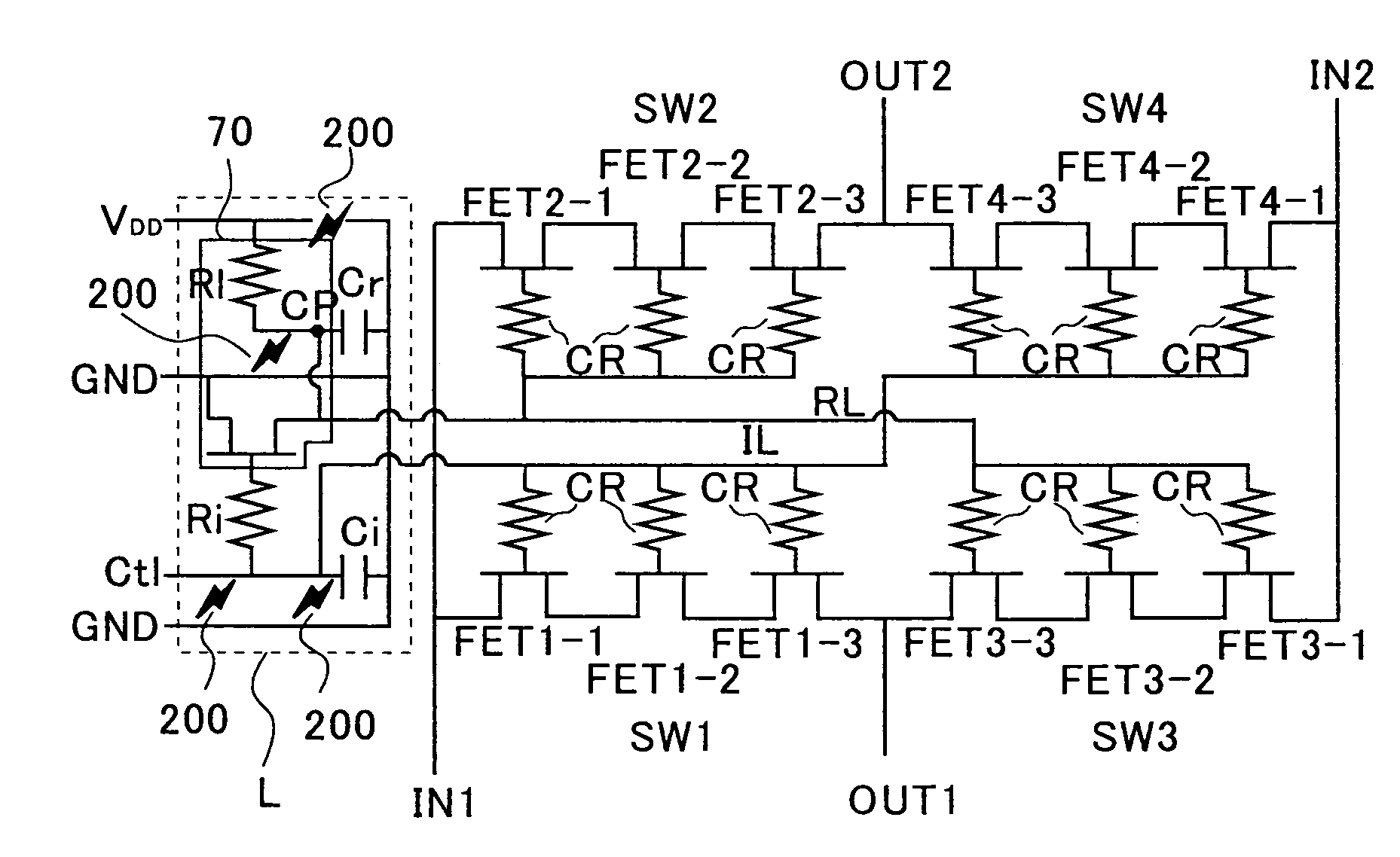
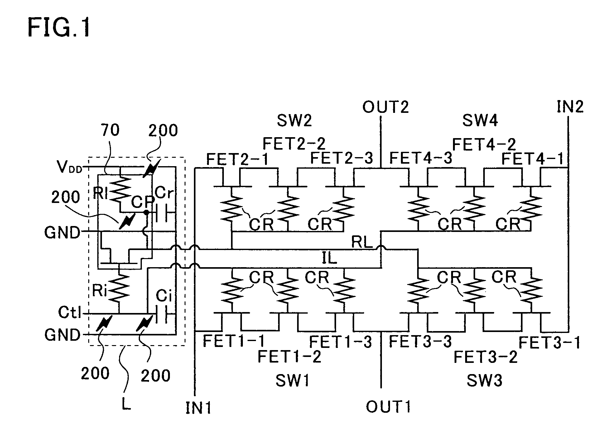
[0032]the present invention will now be explained while referring to FIGS. 1 to 8. FIG. 1 is a circuit diagram showing an example DPDT (Double Pole Double Throw) switching MMIC that includes four switching elements, each of which is formed by connecting a plurality of FETs.

[0033]The DPDT is a switching MMIC that is employed, for example, for a CDMA (Code Division Multiple Access) mobile phone, and includes: first to fourth switching elements SW1, SW2, SW3 and SW4; two first RF ports (first common input terminal IN1 and second common input terminal IN2); and two second RF ports (first common output terminal OUT1 and second common output terminal OUT2). In this arrangement, a SPDT switch, constituted by the first and second switching elements SW1 and SW2, and another SPDT switch, constituted by the third and fourth switching elements SW3 and SW4, are connected by the second RF ports.

[0034]The switching elements SW1, SW2, SW3 and SW4 are FET groups, each of which is formed by connectin...

second embodiment

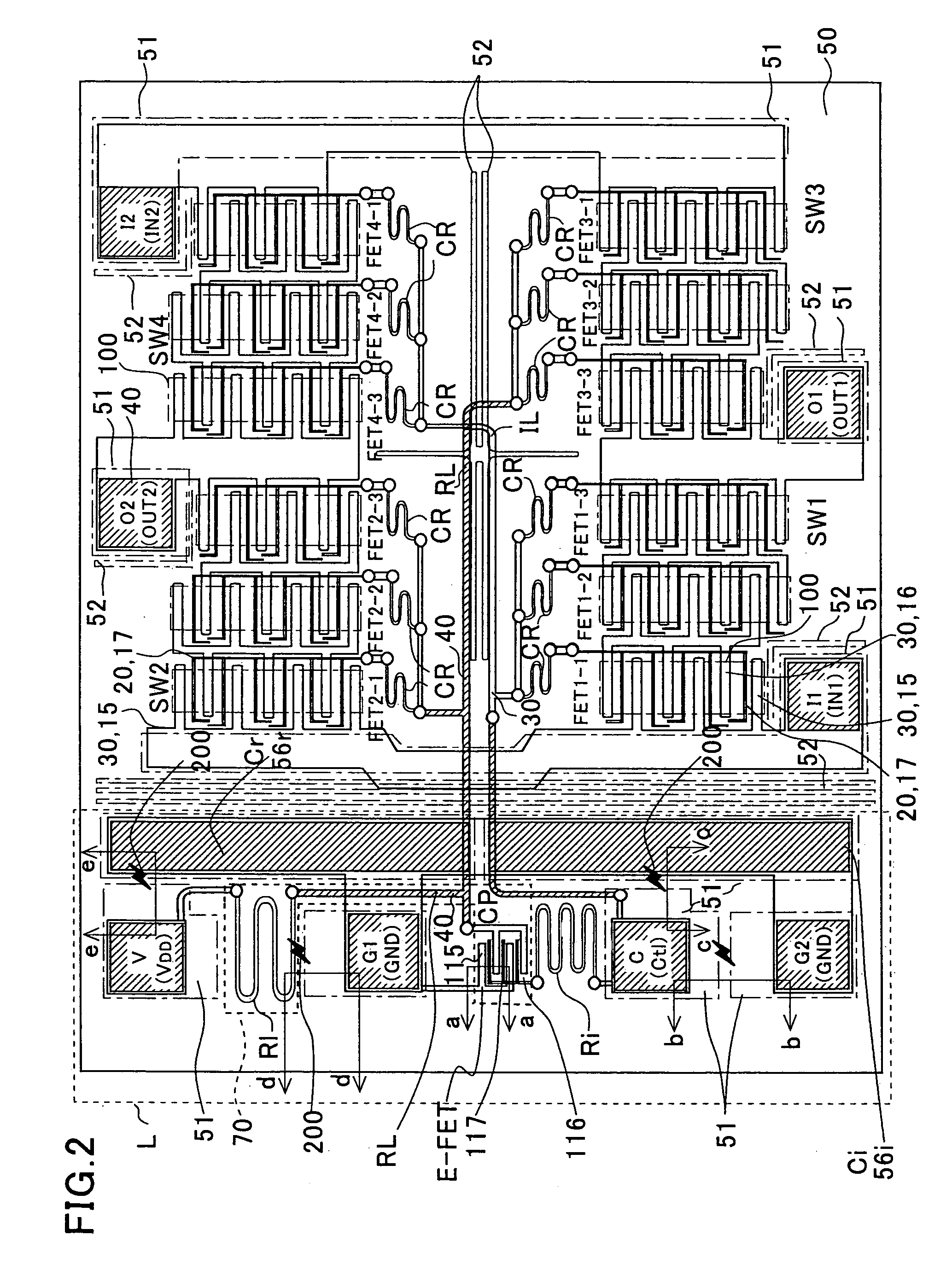
[0123]the present invention will now be described while referring to FIGS. 9 and 10. FIG. 9 is a circuit diagram, and FIG. 10 is a plan view.

[0124]The second embodiment is a case wherein no second ground terminal pad G2 is provided. Lower electrode 55i of capacitor Ci and lower electrode 55r of capacitor Cr are continuous and are connected to first ground terminal pad G. That is, logic circuit L normally operates when the second ground terminal pad G2 of the first embodiment (FIG. 2) is not provided. According to the second embodiment, the protecting element 200 (FIG. 5) indicated by a line b-b in FIG. 2 is not connected. However, by employing the protecting element 200 (FIG. 6), indicated by a line c-c in FIG. 2, devices between control terminal Ctl and ground terminal GND can be protected.

[0125]Since other components are the same as those in the first embodiment, no further explanation for them will be given.

third embodiment

[0126]the present invention will now be explained while referring to FIGS. 11 to 14. FIG. 11 is a circuit diagram showing a switching circuit device, FIG. 12 is a plan view of a switching circuit device, FIGS. 13A and 13B are cross-sectional views of devices that constitute an inverter, and FIG. 14 is a cross-sectional view of a protecting element.

[0127]According to the third embodiment, inverter 70 is called an E / D type DCFL (Direct Coupled FET Logic) wherein a depletion type FET (hereinafter referred to as a D-FET) is connected to an E-FET.

[0128]As shown in FIG. 11, via inverted signal line RL, the D-FET that serves as a load element is connected in series to the E-FET that performs switching. Gate electrodes of the E-FET are connected to control terminal Ctl, and the gate electrodes and source electrode of the D-FET are connected to drain electrode of the E-FET. Drain electrode of the D-FET is connected to power supply terminal VDD.

[0129]As shown in FIG. 12, the inverted signal l...


PUM


Abstract

Protecting elements are respectively connected between a control terminal Ctl and a ground terminal GND of a logic circuit L, between a point Cp and a ground terminal GND, and between a power supply terminal VDD and a ground terminal GND thereof. With this, an E-FET, constituting an inverter 70, and capacitors Ci and Cr can be protected from electrostatic breakdown due to external static electricity. Since the protecting element can be constituted by requisite components for the logic circuit, an additional step or structure is not especially required to provide the protecting element.

Description

BACKGROUND OF THE INVENTION[0001]1. Field of the Invention[0002]The present invention relates to a compound semiconductor switching circuit device, and relates particularly to a compound semiconductor switching circuit device that protects from electrostatic breakdown a logic circuit provided for a switching circuit device.[0003]2. Related Background Art[0004]In many cases, mobile communication devices, such as mobile phones, employ a microwave frequency in a GHz band, and a switching element for switching these high frequency signals tends to be employed for an antenna switching circuit or a transmission / reception switching circuit. A field-effect transistor (hereinafter referred to as an FET) that employs gallium•arsenide (GaAs) is frequently employed as such a switching element, and because of this trend, and developments of monolithic microwave integrated circuits (MMICs) have been proceeded, in which the switching circuits are integrated.[0005]For a conventional compound semico...

Claims


Application Information

Patent Timeline
Patent Type & Authority Patents(United States)
IPC IPC(8): H03K5/08
CPCH01L21/8252H01L27/0266H01L27/0605H01L29/7785H01L21/02H01L21/18
Inventor ASANO, TETSUROKUSAKA, YUICHISAKAKIBARA, MIKITOISHIHARA, HIDETOSHI
Owner SEMICON COMPONENTS IND LLC
Why Eureka
Try Eureka