Liquid crystal driving circuit and load driving circuit

Inactive Publication Date: 2008-04-15
KK TOSHIBA
View PDF11 Cites 1 Cited by
  • Summary
  • Abstract
  • Description
  • Claims
  • Application Information

AI Technical Summary

Benefits of technology

[0036]Additionally, there is provided a load driving circuit configured to selectively drive m (m being an integer of 1 or more) pieces of loads based on an output of an operationa

Problems solved by technology

Since there is only a limited space in a cellular phone, a large-capacitance battery cannot be mounted, and power consumption of a circuit in the phone needs to be reduced as much as possible.
Therefore, the source driver IC having m pieces of driving output terminals always operate m (e.g., 384 or 420) pieces of buffer amplifiers, thereby increasing the power consumption.
However, since the display apparatus of FIG. 12 always selects the grayscale number in accordance with the input image signal, a processing burden in the grayscale conversion / buffer control circuit 71 increases.
Particularly, when the input image signal frequently changes, e.g. a moving picture, the power consumption of the grayscale conversion / buffer control circuit 71 possibly increases.
Moreover, a memory for storing at least one frame of input image signals is necessary, and it is difficult to miniaturize the circuit.
Therefore, a high-precision A / D converter is required, thereby increasing a component cost.
However, when the display apparatus of FIG. 12 is used for the cellular phone, the power consumption of the grayscale conversion / buffer control circuit 71 does not decrease even in the waiting state, and as a result, a waiting time is shortened.
When m is larger, there is a problem that the phase margin is further reduced, and oscillation easily occurs.

Method used


Image

  • Liquid crystal driving circuit and load driving circuit
  • Liquid crystal driving circuit and load driving circuit
  • Liquid crystal driving circuit and load driving circuit

Examples


first embodiment

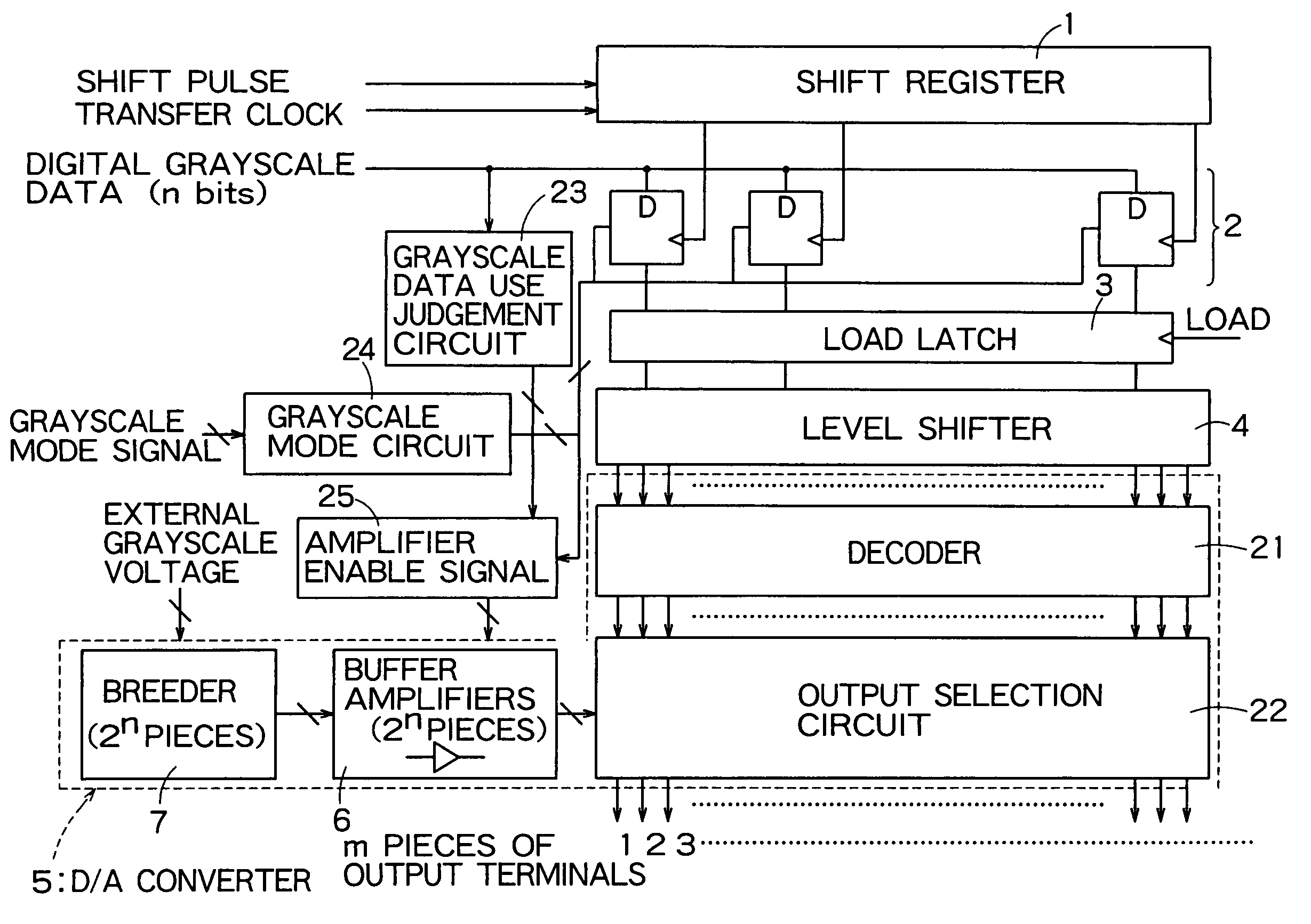
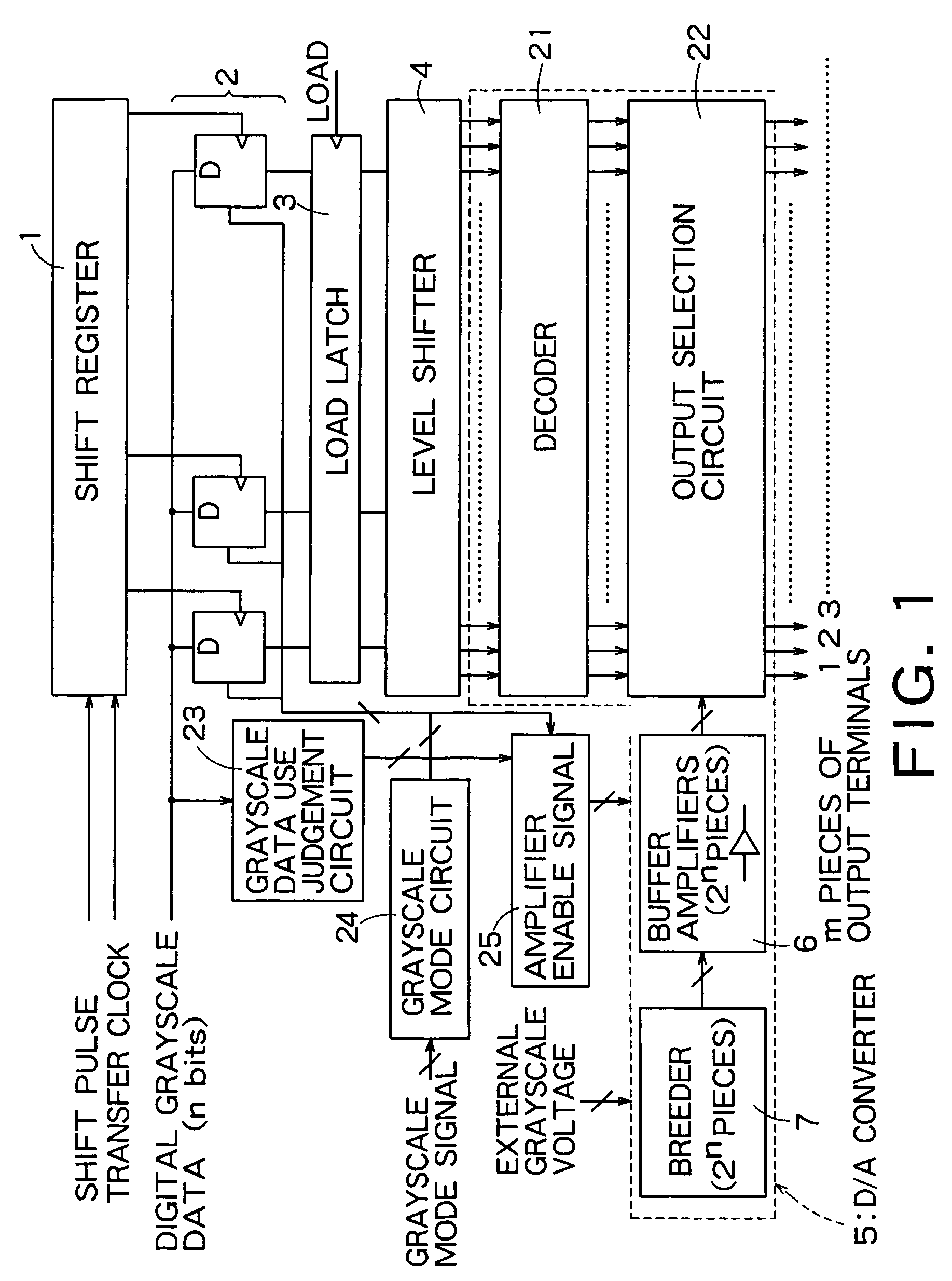
[0059]FIG. 1 is a block diagram showing a schematic configuration of a first embodiment of the liquid crystal driving circuit according to the present invention, and shows a configuration of a signal line driving section. In FIG. 1, constituents common to those of FIG. 11 are denoted with the same reference numerals, and mainly a different respect will be described hereinafter.

[0060]Similarly as FIG. 11, the liquid crystal driving circuit of FIG. 1 includes a shift register 1, a plurality of data latch circuits (first latch circuits) 2, a load latch circuit (second latch circuit) 3, a level shifter 4, a decoder 21, an output selection circuit 22, a breeder (reference voltage generation circuit) 7, and a buffer amplifier 6.

[0061]A D / A converter 5 is composed of the buffer amplifier 6, breeder 7, decoder 21 and output selection circuit 22.

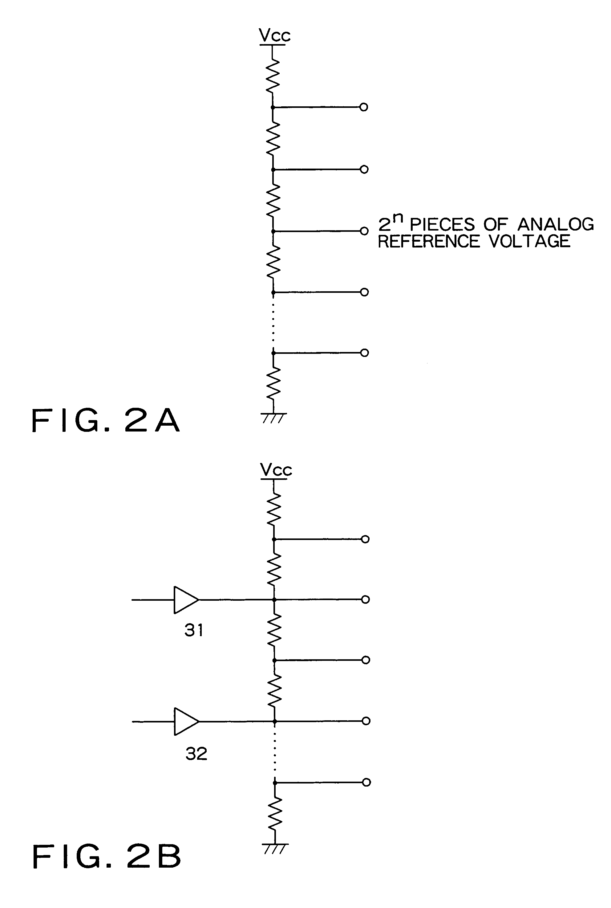
[0062]The breeder 7, for example, as shown in FIG. 2A, divides a voltage between two supply voltages (a power supply voltage and GND voltage) by a p...

second embodiment

[0090]In a second embodiment, a peripheral configuration of the buffer amplifier 6 is devised to shorten a settling time.

[0091]Since the second embodiment is similar to the first embodiment except the peripheral configuration of the buffer amplifier 6, description is omitted.

[0092]FIG. 7 is a circuit diagram showing the peripheral configuration of the buffer amplifier 6. Additionally, when the buffer amplifier 6 is composed of the first and second gain stages 41, 42 as shown in FIG. 5, each of the first and second gain stages 41, 42 is constituted as shown in FIG. 7.

[0093]The buffer amplifier 6 of FIG. 7 includes an operational amplifier constituted of two gain stages 51, 52, and resistors R1 to RN and switches SW1 to SWN are connected in series between the output terminal of the second gain stage (output gain stage) 52 and respective loads.

[0094]The switches SW1 to SWN correspond to analog switches (not shown) in the output selection circuit 22, and the resistors R1 to RN are conne...

third embodiment

[0103]In a third embodiment, a dummy load circuit is added to the buffer amplifier 6 of the second embodiment.

[0104]FIG. 9 is a circuit diagram showing the peripheral configuration of the buffer amplifier 6 of the third embodiment. In the configuration, a dummy load circuit 61 is added to the output terminal of the output gain stage 52 of FIG. 7. The dummy load circuit 61 is composed of connecting a resistor Rd, switch SWd and capacitor Cd in series.

[0105]The second embodiment is on the assumption that at least one of the switches SW1 to SWN connected to the load is turned on. However, when all the switches SW, to SWN are turned off, the operation of the buffer amplifier 6 becomes unstable, and oscillation possibly occurs.

[0106]On the other hand, the buffer amplifier 6 of FIG. 9 turns on the switch SWd in the dummy load circuit 61, when all the switches SW1 to SWN connected to the load a returned off. If the time constant of the resistor Rd and capacitor Cd in the dummy load circuit...


PUM


Abstract

There is disclosed a liquid crystal driving circuit configured to supply an analog voltage in accordance with digital grayscale data to each of a plurality of signal lines, said circuit comprising: a reference voltage generation circuit configured to output analog reference voltages corresponding to each of said digital grayscale data; a plurality of buffer amplifiers configured to individually perform buffering of said respective analog reference voltages; a grayscale mode circuit configured to determine a grayscale number of said digital grayscale data based on a grayscale mode signal supplied from the outside; and an amplifier enable circuit configured to set each of said plurality of buffer amplifiers to an enable state or a disable state based on an output signal of said grayscale mode circuit.

Description

CROSS REFERENCE TO RELATED APPLICATIONS[0001]This application is a division and claims the benefit of priority under 35 USC §120 from U.S. application Ser. No. 09 / 964,465, filed Sep. 28, 2001, and claims the benefit of priority under 35 USC §119 from Japanese Patent Applications No. 2000-300491, filed on Sep. 29, 2000, the entire contents of which are incorporated herein by reference.BACKGROUND OF THE INVENTION[0002]1. Field of the Invention[0003]The present invention relates to a liquid crystal driving circuit in which grayscale display is possible, and a load driving circuit for selectively driving a capacitive load.[0004]2. Related Background Art[0005]Since there is only a limited space in a cellular phone, a large-capacitance battery cannot be mounted, and power consumption of a circuit in the phone needs to be reduced as much as possible. On the other hand, a cellular phone having a color liquid crystal panel has increased.[0006]A conventional source driver IC for driving a liq...

Claims


Application Information

Patent Timeline
IPC IPC(8): G09G3/36G02F1/133G09G3/20
CPCG09G3/3688G09G3/3696G09G3/2011G09G2310/027G09G2330/021G09G2360/16G09G3/36
Inventor SAITO, TETSUYAMINAMIZAKI, HIRONORIITAKURA, TETSURO
Owner KK TOSHIBA
Why Eureka
Try Eureka