Optical coupling device and method for bidirectional data communication over a common signal line

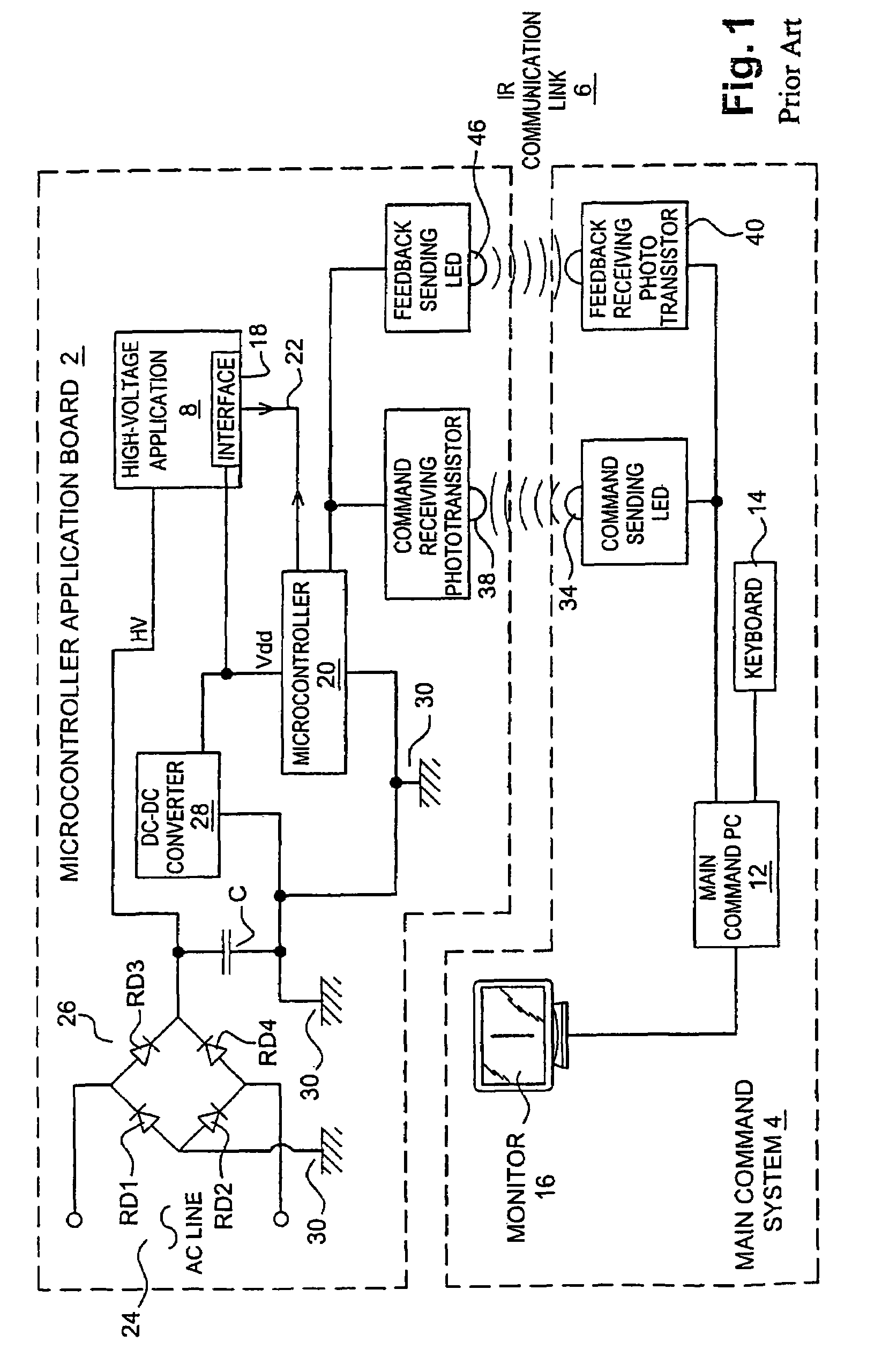
a technology of optical coupling and signal line, which is applied in the direction of optical light guides, counting objects on conveyors, photoelectric discharge tubes, etc., can solve the problems of potential danger either for the user or the circuitry, the inability of opto-isolators to be interposed in the data wire path, and the inability to use opto-isolators

Active Publication Date: 2008-04-15
STMICROELECTRONICS SRL
View PDF3 Cites 95 Cited by
  • Summary
  • Abstract
  • Description
  • Claims
  • Application Information

AI Technical Summary

Problems solved by technology

This type of ground connection would raise a problem if it were attempted to connect the ground of the microcontroller 20 directly to the ground of the main command PC 12 or other part of the main command system 4, since the chassis of the latter could then be at a potential which is dangerous either for a user or for the circuitry.
Under these circumstances, opto-isolators cannot be interposed in the data wire path to obtain the isolation, since they are designed to pass information along one direction only.
Likewise, opto-isolators cannot be used either in applications where a command link may be connected by a single wire or a common group of wires to several addressable sending or receiving units, where each link is joined to an arbitrary number n of open-collector outputs of n respective sending and receiving units via pull-up or pull-down resistors and the signal can be imposed from either end of the link.
However, the circuit of FIG. 3 will fail since whenever one of the units A or B attempts to send data, there is created a lock up situation in which each of the two LEDs 58A and 58B switch on and remain on.

Method used


Image

  • Optical coupling device and method for bidirectional data communication over a common signal line
  • Optical coupling device and method for bidirectional data communication over a common signal line
  • Optical coupling device and method for bidirectional data communication over a common signal line

Examples


first embodiment

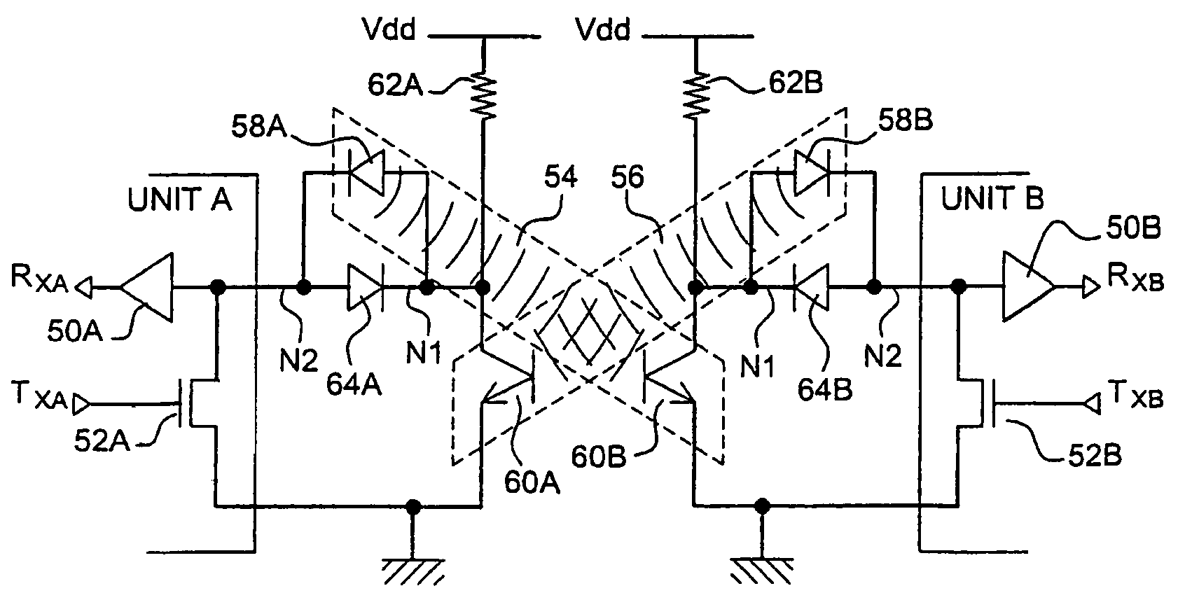
[0093]The circuit diagram of the invention is shown in FIG. 5. The embodiment is based on the same two units A and B as in FIG. 3 communicating by the same protocol and the same internal circuitry as already described in connection with that Fig., notably as regards the buffer 50A / 50B and transmission FET switch 52A / 52B. Accordingly, the two units A and B exchange data using the common bidirectional serial data link DCL as described. Also, a system of two logic type opto-isolators 54 and 56 is present in that common data link DCL to isolate the units A and B.

[0094]In FIG. 5, elements having already been described in the context of FIG. 3 have the same reference numerals as in FIG. 3 and, for the sake of conciseness, shall not be described again insofar as they have the same form or function, it being understood that the above description of features of FIG. 3 common to FIG. 5 are hereby incorporated by reference.

[0095]The circuit of FIG. 5 differs from that of FIG. 3 notably in that...

second embodiment

[0129]The circuit of FIG. 7 shows this variant implemented with the In this case, additional pull-up resistors 662A / 662B and the resistors 66A / 66B form a voltage divider between Vdd and ground when the phototransistor of their respective unit is conducting (ignoring VCEsat of that phototransistor).

[0130]Now, with such a circuit configuration, the additional pull-up resistors 662A / 662B can be placed physically either:[0131]outside the unit A or B with which they are associated, whereupon they can be biased by a power supply serving for the opto-isolators 54 and 56, which is independent of the power supply for the unit A or B itself. This configuration is shown inFIG. 8A for the case of unit A, or[0132]within the unit A or B with which they are associated, for instance if the additional pull-up resistors 662A / 662B are already present on chip. This configuration is shown in FIG. 8B for unit A. In this case, the same power supply of the unit A or B serves to bias both the pull-up resis...

third embodiment

[0134]FIG. 9 shows the invention, based on the embodiment of FIG. 3, with a connection at each end to a totem-pole coupler circuit. Most phototransistors have open collector outputs, but in very-high speed opto-coupling applications, totem-pole output photodetectors can be used instead. This variant calls for a modification of the previous circuit diagram, since the pull-up resistor is replaced by an active component, as illustrated.

[0135]Specifically, FIG. 9 shows the circuit configuration simply for unit A, it being understood that the configuration is the same for unit B.

[0136]At the level of the head-to-tail Schottky diode 64A and LED 58A, there is added a series resistor 70 having a first terminal connected to the anode of LED 58A and its second terminal connected to the cathode of Schottky diode 64A. Series resistor 70 serves to limit the current through LED 58A. In the previous embodiment, the current through that LED is limited by the pull-up resistor, absent from this circu...


PUM


Abstract

Optical coupling device operates over a bidirectional data link between at least first and second communicators, each communicating data along a common wire of the data link. The device includes at least first and second optical couplers, each including a photon flux source and a photon flux detector. The photon flux source of the first and second optical couplers, respectively, is commanded by the first and second communicator, respectively. The photon flux detector of the first and second optical coupler, respectively, produces a signal on the data link at the first and second communicator, respectively, in response to the photon flux source of the second and first optical coupler, respectively, from the second and first communicator, respectively. An inhibitor inhibits the photon flux source of the second and first optical coupler, respectively, in response to an activation of the photon flux source of the first and second optical coupler, respectively.

Description

BACKGROUND OF THE INVENTION[0001]1. Field of the Invention[0002]The present invention relates to an optical coupling device and method operative in a bidirectional data transmission link. An optical coupling serves to provide voltage isolation, also known as galvanic isolation, between communicating devices which are located at respective ends of a data transmission link. Generally, an optical data coupling is implemented with one or several opto-isolators, each comprising a light emitting diode (LED) and a phototransistor operating in tandem. The separation between the LED and phototransistor defines an electrically isolated optical path. The LED acts as a photon flux source and is activated by the sending device to produce a signal carrying modulation. This modulation by illumination is detected by the phototransistor, which acts as a photon flux detector, connected the receiving device. In this way, a suitable modulated signal applied to the LED by a sending device can be reprodu...

Claims


Application Information

Patent Timeline
Patent Type & Authority Patents(United States)
IPC IPC(8): H04B10/00H04B10/24
CPCH04B10/2503H04B10/801H04B10/2589
Inventor ONDE, VINCENTTEISSIER, MAXIME
Owner STMICROELECTRONICS SRL
Why Eureka
Try Eureka