Stacked embedded leadframe

a leadframe and leadframe technology, applied in the field of electronic component packaging, can solve the problems of large impedance associated with the bond wire, place a fundamental restriction on the minimum size of the electronic component package, and affect so as to minimize the impedance, simplify manufacturing, and maximize the reliability of the electrical connection

Inactive Publication Date: 2008-04-22
AMKOR TECH SINGAPORE HLDG PTE LTD
View PDF396 Cites 97 Cited by
  • Summary
  • Abstract
  • Description
  • Claims
  • Application Information

AI Technical Summary

Benefits of technology

[0011]Thus, in accordance with this embodiment of the present invention, the bond pads and the lower mounting portions of the leads are directly connected to the corresponding vias. Stated another way, the bond pads of the electronic component and lower mounting portion of each lead in the plurality of leads in the leadframe are electrically connected to the corresponding vias without the use of a solder, e.g., without the use of flip chip bumps, and without the need to form a solder wetting layer, e.g., a nickel / gold layer, on the bond pads or on the leads of the leadframe. This maximizes the reliability of the electrical connection between vias and the bond pads / leads, while at the same time minimizes impedance.
[0012]Further, since the dielectric strip is directly attached to the electronic component and the bond pads are directly connected to the corresponding vias, the use of an underfill material is obviated. This simplifies manufacturing, enhances reliability, and thus reduces cost.
[0013]Further still, the embedded leadframe permits stacking of additional electronic component packages and / or electronic components thereon. The stacking capability provides a smaller, refined geometry of individual electronic component packages and of an overall stacked assembly of multiple electronic component packages and / or electronic components.

Problems solved by technology

In the wirebond configuration described above, however, traces of the substrate were fanned out around the integrated circuit chip, which placed a fundamental restriction on the minimum electronic component package size.
Further, a large impedance was associated with the bond wires.
However, the flip chip bumps between the bond pads of the integrated circuit chip and traces on the substrate were subject to significant stress, e.g., due to differential thermal expansion between the integrated circuit chip and the substrate.
Thus, failure of the flip chip bumps often occurred which decreased yield and thus increased the cost of the electronic component package.
However, the application of the underfill material required an additional manufacturing step, which increased the cost of the electronic component package.

Method used


Image

  • Stacked embedded leadframe
  • Stacked embedded leadframe
  • Stacked embedded leadframe

Examples


Embodiment Construction

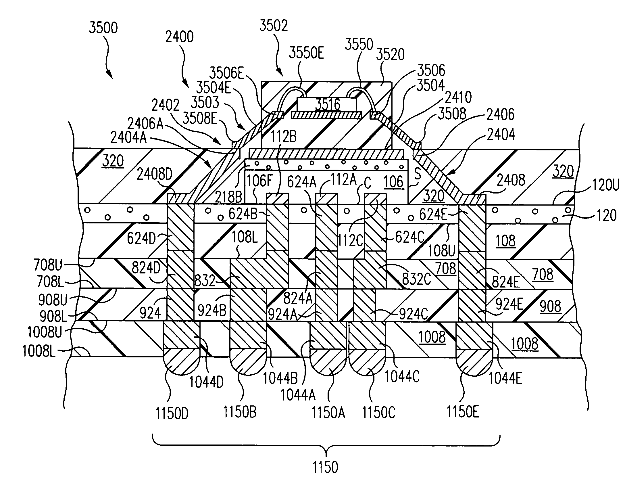
[0030]In accordance with one embodiment of the present invention, referring to FIG. 25, a method of forming an electronic component package includes coupling a front surface 106F of a first electronic component 106 to a first surface 108U of a first dielectric strip 108, first electronic component 106 comprising bond pads 112 on first surface 106F of first electronic component 106.

[0031]A leadframe 2402 is coupled to first surface 108U of first dielectric strip 108. Leadframe 2402 comprises, for example, a support plate 2410 and a plurality of leads 2404. Each lead 2404 in the plurality of leads 2404 has a terminal portion 2406 and a lower mounting portion 2408. Lower mounting portion 2408 is connected to first surface 108U of first dielectric strip 108.

[0032]A package body 320 (FIG. 26) is formed by encapsulating first electronic component 106 and partially encapsulating leadframe 2402 such that portions of leadframe 2402 are exposed in a principal surface 320U of package body 320....


PUM


Abstract

A method of forming a stackable embedded leadframe package includes coupling an electronic component having bond pads to a substrate; coupling on the substrate a leadframe having a plurality of leads, each lead having a lower mounting portion; encapsulating the electronic component and partially encapsulating the leadframe; singulating each lead; forming via apertures through the substrate to expose the bond pads and the lower mounting portions; and filling the via apertures with an electrically conductive material to form vias electrically coupled to the bond pads and to the lower mounting portions. This permits stacking of electronic components in a small geometry.

Description

RELATED APPLICATIONS[0001]This application is a continuation-in-part of U.S. Ser. No. 11 / 123,605, filed May 5, 2005, issued as U.S. Pat. No. 7,192,807, which is a continuation of U.S. Ser. No. 10 / 291,050, filed Nov. 8, 2002, issued as U.S. Pat. No. 6,905,914 and this application is a continuation-in-part of U.S. Ser. No. 10 / 868,244, filed Jun. 15, 2004, issued as U.S. Pat. No. 7,190,062. This application incorporates herein each of the foregoing applications in their entirety.BACKGROUND OF THE INVENTION[0002]1. Field of the Invention[0003]The present invention relates generally to the packaging of electronic components. More particularly, the present invention relates to an electronic component package and method of fabricating the same.[0004]2. Description of the Related Art[0005]One form of an electronic component package included an electronic component such as an integrated circuit chip mounted to a substrate. For example, in a wirebond configuration, bond wires were used to for...

Claims


Application Information

Patent Timeline
Patent Type & Authority Patents(United States)
IPC IPC(8): H01L21/00H01L23/495
CPCH01L24/19H01L23/3128H01L23/49811H01L24/97H01L25/105H01L2224/32245H01L2224/48247H01L2224/0401H01L2924/10253H01L2225/1094H01L2225/1035H01L2224/16225H01L2924/01033H01L2924/01019H01L2924/01006H01L24/48H01L2924/3011H01L2924/19041H01L2924/15311H01L2924/14H01L2924/01322H01L2924/01082H01L2924/01079H01L2924/01078H01L2924/01075H01L2224/73265H01L2224/04105H01L2224/20H01L2224/48091H01L2224/83192H01L2224/92144H01L2224/97H01L2924/01013H01L2924/01027H01L2924/01029H01L2924/01047H01L2224/82H01L2924/00014H01L2924/00012H01L2924/00H01L24/73H01L2924/181H01L24/49H01L2224/49175H01L2224/45099H01L2224/45015H01L2924/207
Inventor HUEMOELLER, RONALD PATRICKRUSLI, SUKIANTOHINER, DAVID JON
Owner AMKOR TECH SINGAPORE HLDG PTE LTD
Why Eureka
Try Eureka