
Active smart antenna system and fabrication method thereof

Inactive Publication Date: 2008-04-29
LG ELECTRONICS INC
View PDF31 Cites 13 Cited by
  • Summary
  • Abstract
  • Description
  • Claims
  • Application Information

AI Technical Summary

Benefits of technology

[0018]Therefore, an object of the present invention is to provide an active smart antenna system capable of reducing a fabrication cost by simultaneously implementing a phase shifter, an antenna, and a low noise amplifier on one high resistance substrate, and a fabrication method thereof.
[0019]Another object of the present invention is to provide an active smart antenna system capable of improving a quality thereof by simultaneously implementing a phase shifter, an antenna, and a low noise amplifier on one high resistance substrate, and a fabrication method thereof.

Problems solved by technology

However, since the passive smart antenna system has a large size and an expensive fabrication cost, a spread ratio thereof is not high.
According to this, a development of an active smart antenna system having a relatively small size and a cheap fabrication cost is absolutely required.
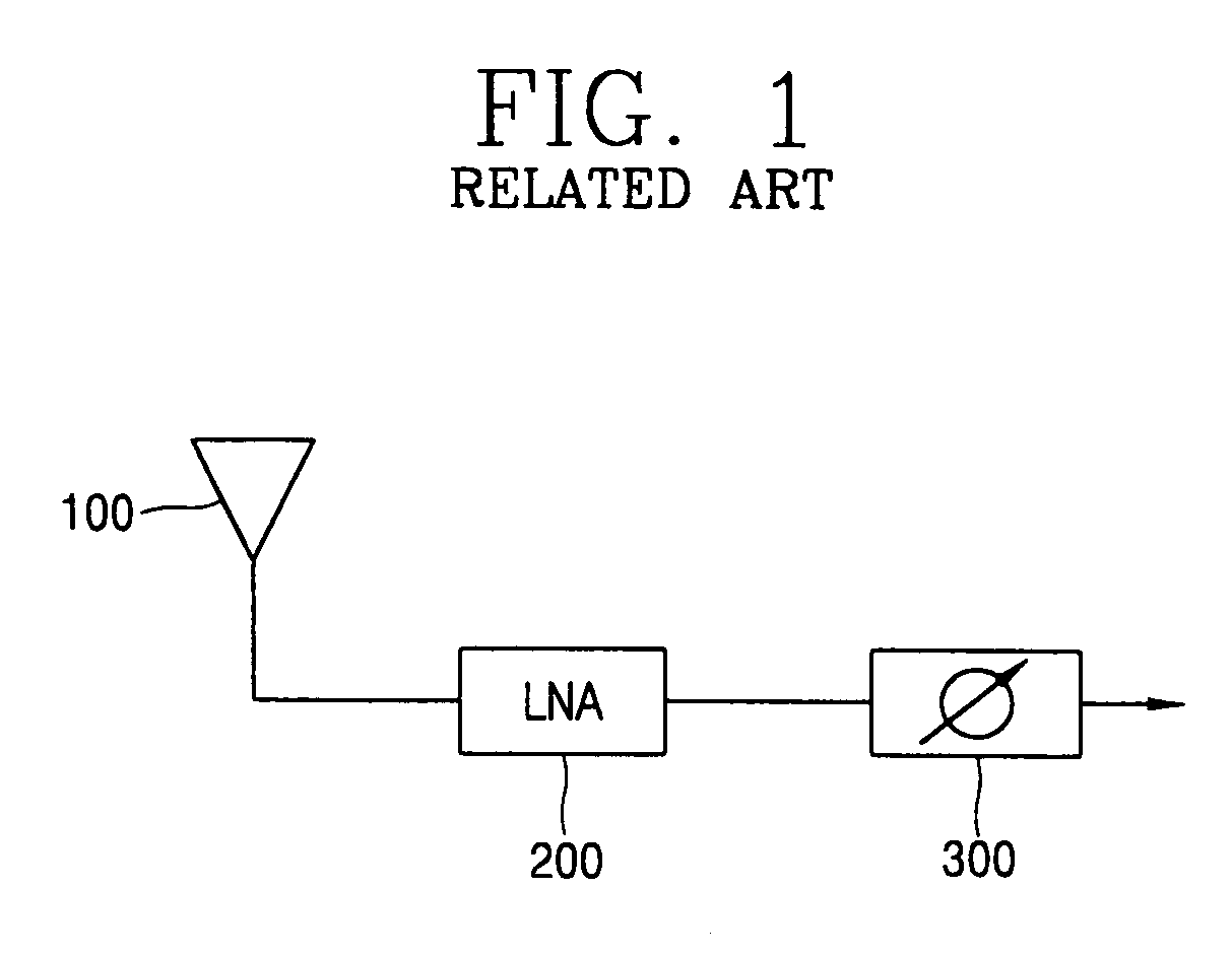
Among the components constituting the active smart antenna system, the phase shifter 300 occupies a space the most and requires the most expensive cost.
According to this, a fabrication cost is increased and a quality factor of the inductor (for example 8˜13) is low thus not to be able to anticipate a high quality.
Therefore, in the active smart antenna system, a lead for bonding the fabricated phase shifter 300 on the PCB is required, thereby increasing an entire size and deteriorating a quality factor of the inductor.
As aforementioned, according to the active smart antenna system in accordance with the related art, the phase shifter is fabricated by the MMIC technology, a semiconductor process, thereby increasing a fabrication cost.
Also, according to the active smart antenna system in accordance with the related art, the phase shifter is fabricated by the MMIC technology, a semiconductor process, thereby lowering a quality thereof.

Method used


Image

  • Active smart antenna system and fabrication method thereof
  • Active smart antenna system and fabrication method thereof
  • Active smart antenna system and fabrication method thereof

Examples


Embodiment Construction

[0028]Reference will now be made in detail to the preferred embodiments of the present invention, examples of which are illustrated in the accompanying drawings.

[0029]Hereinafter, an active smart antenna system capable of reducing an entire size thereof, reducing a fabrication cost thereof, and improving a quality thereof by simultaneously implementing a phase shifter, an antenna, and a low noise amplifier on one high resistance substrate, and a fabrication method thereof will be explained with reference to the attached drawings.

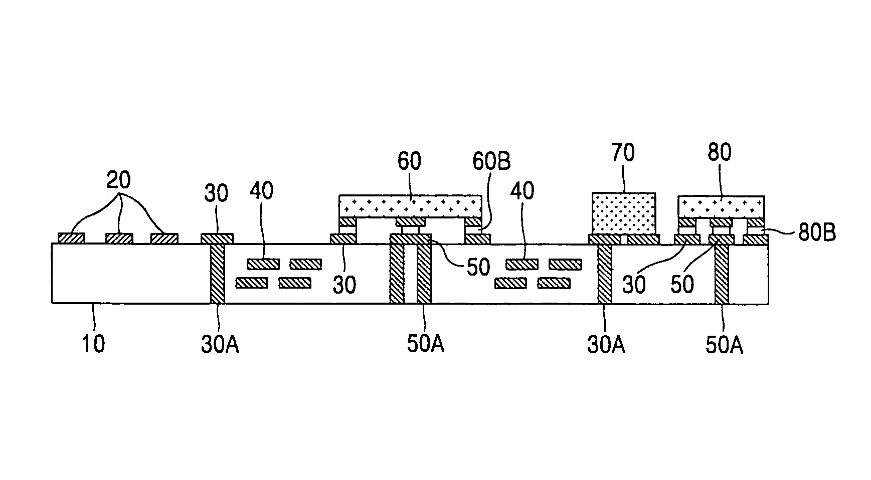
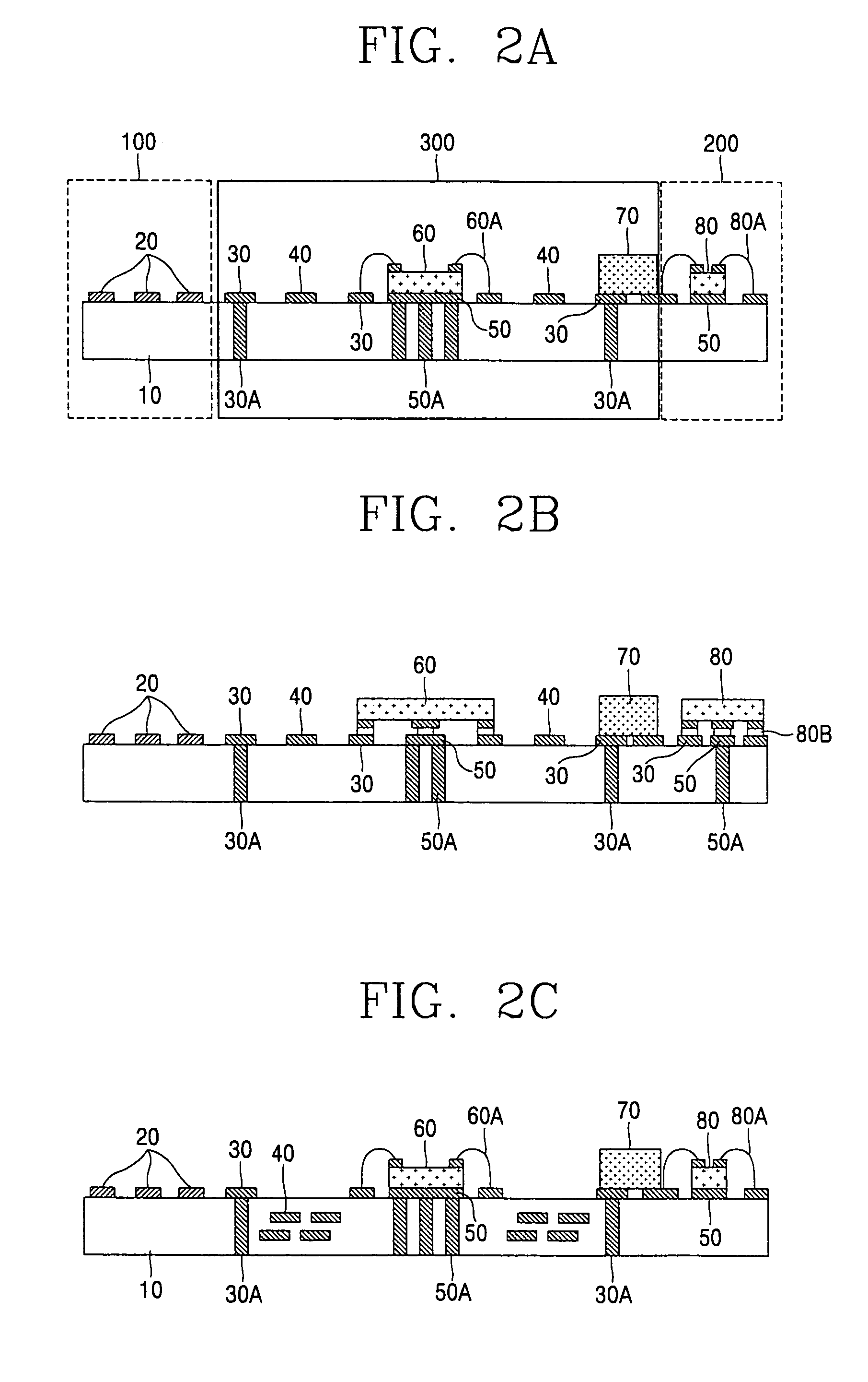
[0030]FIGS. 2A to 2I are sectional views showing various structures of the active smart antenna system according to the present invention.

[0031]As shown in FIG. 2A, the active smart antenna system according to the present invention comprises: an antenna 100 for receiving a signal; a low noise amplifier (LNA) 200 for amplifying a signal received through the antenna so as to minimize a noise generation; and a phase shifter 300 for controlling a phase of the si...


PUM


Abstract

Disclosed are an active smart antenna system and a method thereof. The system comprises: an antenna for receiving a signal; a low noise amplifier for amplifying a signal received through the antenna so as to minimize a noise generation; and a phase shifter for controlling a phase of the amplified signal. The antenna, the low noise amplifier, and the phase shifter are formed on one high resistance substrate.

Description

CROSS-REFERENCE TO RELATED APPLICATIONS[0001]Pursuant to 35 U.S.C. § 119(a), this application claims the benefit of earlier filing date and right of priority to the Korean Application No. 10-2003-0016185, filed on Mar. 14, 2003, the content of which is hereby incorporated by reference herein in its entirety.BACKGROUND OF THE INVENTION[0002]1. Field of the Invention[0003]The present invention relates to an antenna system, and more particularly, to an active smart antenna system and a fabrication method thereof.[0004]2. Description of the Related Art[0005]Generally, a smart antenna system is a core component necessary in a next generation communication system, and is used at a high frequency band such as a mobile vehicle satellite broadcasting / communication, a military communication, and etc. The smart antenna system can be positioned at a base station or a mobile terminal according to an arrangement size of an antenna. The smart antenna system can accommodate a large number of users,...

Claims


Application Information

Patent Timeline
IPC IPC(8): H01Q1/38H01Q21/00H01Q23/00H04B1/18
CPCH01Q1/38H01Q21/00H01Q23/00H01L2224/73265H01L2224/48091H01L2224/16225H01L2924/00014H01L2224/32225H01L2224/48227H01L2224/05573H01L2224/05568H01L2924/00H01L2224/05599
Inventor PARK, JAE YEONG
Owner LG ELECTRONICS INC
Learn More