Display device employing electrophoretic migration

a display device and electrophoretic technology, applied in static indicating devices, non-linear optics, instruments, etc., can solve the problems of affecting electrophoretic movement, lowering display contrast, deteriorating display contrast, etc., to prevent the migration of charged electrophoretic particles toward the second substrate 2 and simplify the manufacturing process.

Inactive Publication Date: 2008-04-29
KAISHA CANON KABUSHIKI
View PDF4 Cites 67 Cited by
  • Summary
  • Abstract
  • Description
  • Claims
  • Application Information

AI Technical Summary

Benefits of technology

[0050]FIGS. 6(a) and 6(b) show the display electrode 7 that are in a regular hexagon and a square, respectively, and define pixels in a regular hexagon and a square, respectively. The partition walls 5 are disposed to surround the pixel. An aperture in a shape similar to the shape of the pixel is provided in the display electrode 7 at the center of the pixel, and the collector electrode 6 is disposed in the aperture. Although not shown, the collector electrode 6 can be extended under the display electrode 7. The aperture may not necessarily be in a figure similar to that of the pixel, and the collector electrode 6 may preferably be spaced generally equidistant from the partition wall electrodes 5 that surround the collector electrode 6. FIG. 6(c) shows an example in which the pixel is in an oblong configuration. This configuration may be used, for example, in a color display apparatus in which R / G / B pixels are disposed side by side. Two collector electrodes 6 are disposed in each pixel, and each of the collector electrodes 6 is in an oblong configuration whose longer sides extends in the same direction as that of the pixel, such that each of the collector electrodes 6 is spaced generally equidistant from the partition wall electrodes. FIGS. 6(a) through 6(c) show examples in which the collector electrode is disposed at a position generally equidistant from the partition wall electrodes. However, in order to create the effects of the invention, the collector electrode only needs to be provided to reinforce the electric field at least in places farthest from the partition walls, and needs not necessarily be equidistant from the partition walls. FIGS. 7(a) through 7(c) show examples in which a collector electrode is provided in an area that includes the center of the pixel which is located farthest from the partition walls, and extends in elsewhere from the center of the pixel.
[0051]The pixel shown in FIG. 7(a) has the same pixel configuration as that of the pixel shown in FIG. 6(c). Since the electric field of the partition wall electrodes 8 becomes weakest at a center 84 of the pixel, the collector electrode 6 is provided in areas including the center of the pixel and extended sideways. The extended direction and shape of the collector electrode 6 are determined to provide the collector electrode 6 with a sufficient width or an area with which the charged electrophoretic particles can readily gather, and the collector electrode 6 is divided in a manner to divide the pixel into two equal segments in order to minimize as much as possible the difference between the maximum value of the electric field and the minimum value thereof.
[0052]The pixel shown in FIG. 7(b) has the same pixel configuration as that of the pixel shown in FIG. 6(a). The collector electrode 6 is provided in areas including the center of the pixel and in a manner to divide the pixel in two equal segments. The same effects as described above can be obtained with this electrode structure. Since the pixel in this example is in a regular hexagon, the configuration of the collector electrode 6 can be decided to divide the pixel into three or six equal segments. FIG. 7(c) shows an example in which the pixel is divided into six equal segments.
[0053]FIGS. 8(a) and 8(b) and FIGS. 9(a) and 9(b) show other configurations in which the collector electrodes 6 and the partition wall electrodes 5 are formed in one piece. FIG. 8(a) and FIG. 9(a) are plan views of the pixels, and FIG. 8(b) and FIG. 9(b) are cross-sectional views of the pixels taken along lines 8B-8B and 9B-9B, respectively, of the corresponding plan views. In the collector electrodes shown in FIGS. 8(a) and 8(b) and FIGS. 9(a) and 9(b), the collector electrode 6 and the partition wall electrode 5 are connected in a unitary fashion in a region where the collector electrode 6 and the partition wall electrode 5 overlap one another, such as a region A. In this case, since the collector electrode and the partition wall electrode can be formed at once, the manufacturing process can be simplified.
[0054]FIG. 10 shows a still another structure example in which a fourth electrode 10 is provided on the second substrate 2. When the charged electrophoretic particles migrate toward the second substrate 2, and stick to the surface of the second substrate 2, the display contrast is deteriorated. To suppress this phenomenon, a voltage having the same polarity as that of the charged electrophoretic particles may be applied to the fourth electrode 10. As a result, the migration of the charged electrophoretic particles toward the second substrate 2 can be prevented. For example, when the charged electrophoretic particles are charged in a positive polarity, a voltage in the same polarity, i.e., a positive polarity is applied to the fourth electrode 10, such that the migration of the charged electrophoretic particles toward the second substrate 2 is suppressed.
[0055]Next, members that compose the electrophoretic display device in accordance with an embodiment of the present invention will be described.

Problems solved by technology

By so doing, transfer of charges occur due to the coloring agents, which adversely affects electrophoretic movements of the charged electrophoretic particles, and deteriorates the service life and stability of the display device.
Also, when the dielectric liquid is colored, the pigments in the dielectric liquid are adsorbed in the charged electrophoretic particles, which results in a problem of lowered display contrast.
However, the electrophoretic display device described above has the following problems.
For this reason, if, for example, the charged electrophoretic particles on the second electrodes are to be migrated onto the first electrode, many of the charged electrophoretic particles converge on the end sections of the first electrode, and it is difficult for the charged electrophoretic particles to reach the central area of the first electrode.
Also, once the charged electrophoretic particles have moved to the central area of the surface of the first electrode, then it is difficult to migrate the particles to the second electrodes, and the charged electrophoretic particles are fixedly adhered to the central area of the first electrode.
As a result, this causes a major problem of lowered display contrast.
However, by so doing, problems relating to the dielectric strength make the active matrix driving employing switching elements difficult.
Also, in view of the active matrix driving, the conventional electrophoretic display device has another problem.
For this reason, the electric capacity of the display panel is extremely small.

Method used


Image

  • Display device employing electrophoretic migration
  • Display device employing electrophoretic migration
  • Display device employing electrophoretic migration

Examples


embodiment example 1

(Embodiment Example 1)

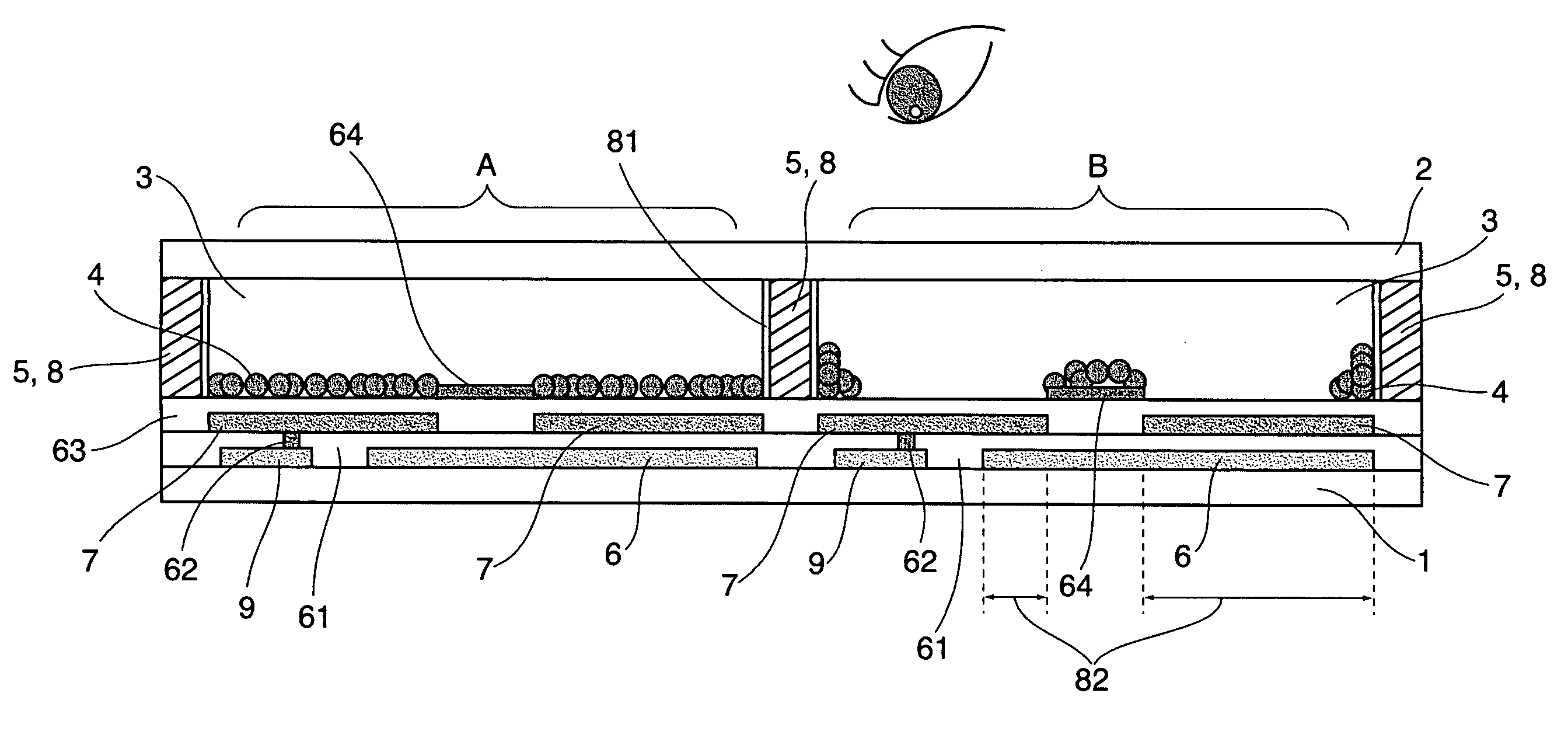
[0065]In accordance with an embodiment example 1, an electrophoretic display device having the structure indicated in FIG. 1 is manufactured. For the sake of simplicity, the following description may be made with reference to a method for manufacturing a single electrophoretic display device for each pixel or two adjacent pixels. However, it is obvious that a plurality of electrophoretic display devices can be manufactured at the same time.

[0066]In the display device of the embodiment example 1, each pixel has a size of 120 μm×120 μm, an area ratio between the collector electrode 6 and the display electrode 7 is 2:8, and the partition wall 5 has a width of 5 μm.

[0067]A glass substrate (1.1 mm thick) is used as the first substrate 1, and a switching element 9, other wirings needed for driving (not shown), an IC, and a collector electrode 6 are formed on the first substrate 1.

[0068]Next, a Si3N4 film as a dielectric layer 61 is formed over the entire surface of t...

embodiment example 2

(Embodiment Example 2)

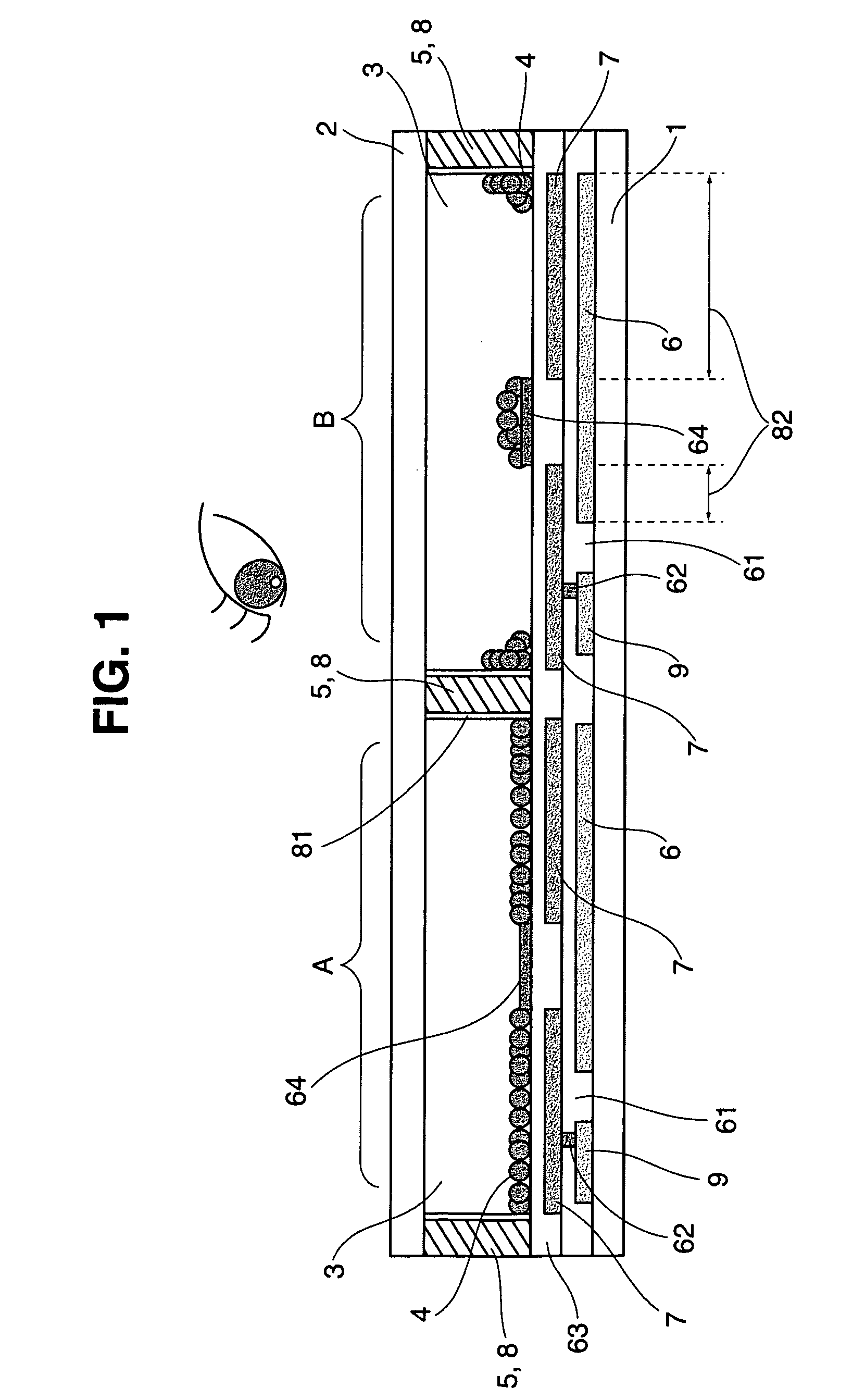
[0075]In accordance with an embodiment example 2, an electrophoretic display device having the structure indicated in FIG. 2(b) is manufactured.

[0076]In the display device of the embodiment example 2, each pixel has a size of 200 μm×200 μm, an area ratio between the collector electrode 6 and the display electrode 7 is 2:8, and the partition wall 5 has a width of 7 μm.

[0077]A stainless foil substrate (260 μm thick) is used as the first substrate 1, and a switching element 9, other wirings needed for driving (not shown), an IC, and a collector electrode 6 are formed on the first substrate 1.

[0078]Next, an acrylic resin layer as a dielectric layer 61 is formed over the entire surface of the first substrate. At the same time, a contact hole 62 for making an electrical contact between the switching element 9 and a display electrode to be formed later is formed in the dielectric layer 61.

[0079]Next, an aluminum (Al) film as a display electrode is formed over the diel...

embodiment example 3

(Embodiment Example 3)

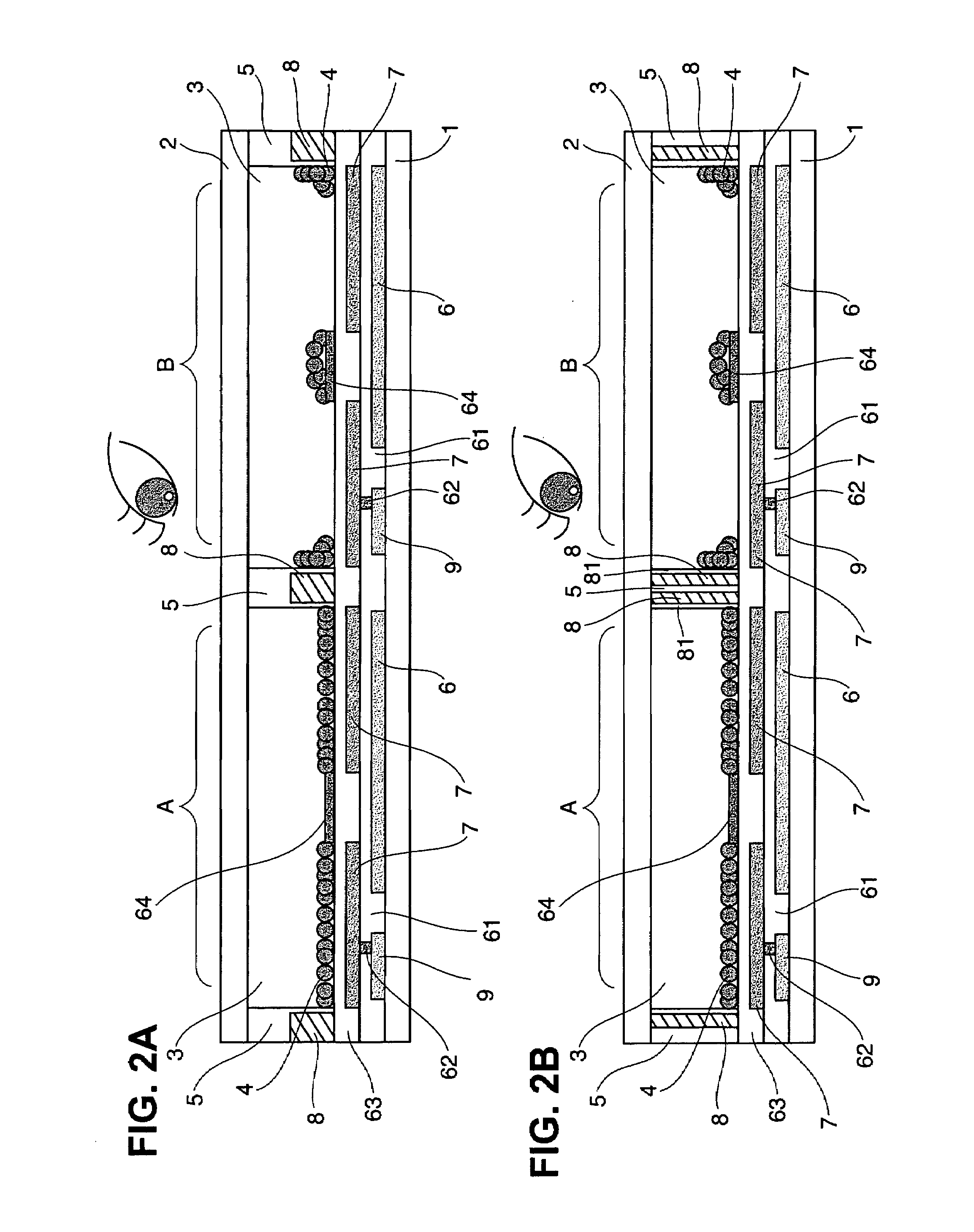
[0085]In accordance with an embodiment example 3, an electrophoretic display device having the structure indicated in FIG. 2(c) is manufactured.

[0086]In the display device of the embodiment example 1, each pixel has a size of 130 μm×130 μm, an area ratio between the collector electrode 6 and the display electrode 7 is 2:8, and the partition wall 5 has a width of 7 μm.

[0087]A glass substrate (1.1 mm thick) is used as the first substrate 1, and a switching element 9, other wirings needed for driving (not shown), an IC, and a collector electrode 6 are formed on the first substrate 1.

[0088]Next, a Si3N4 film as a dielectric layer 61 is formed over the entire surface of the first substrate. At the same time, a contact hole 62 for making an electrical contact between the switching element 9 and a display electrode to be formed later is formed in the dielectric layer 61.

[0089]Next, an aluminum (Al) film as a display electrode is formed over the dielectric layer, and p...


PUM

PropertyMeasurementUnit
heightaaaaaaaaaa
heightaaaaaaaaaa
widthaaaaaaaaaa

Abstract

An electrophoretic display device includes a first substrate and a second substrate disposed opposite each other, a dielectric liquid filled in a gap between the first substrate and the second substrate, a plurality of charged electrophoretic particles dispersed in the dielectric liquid, a first electrode and a second electrode disposed on the first substrate to define a pixel, a partition wall disposed on at least one of the first substrate and the second substrate between adjacent pixels to prevent migration of the charged electrophoretic particles between the adjacent pixels, and a third electrode disposed adjacent to the partition wall. The charged electrophoretic particles migrate at least between a surface of the first electrode and a surface of the second electrode, and between the surface of the first electrode and a side surface of the partition wall where the third electrode is disposed to thereby switch displays.

Description

BACKGROUND OF THE INVENTION[0001]1. Field of the Invention[0002]The present invention relates to an electrophoretic display device wherein images or patterns are formed on the display device by electrophoretic migration of charged particles.[0003]2. Related Background Art[0004]The amount of information that can be handled by each individual is rapidly increasing due to the remarkable advancement in the digital technology. Along with this tendency, thin display devices with low power consumption as information output devices have been extensively developed.[0005]As one of such display devices, an electrophoretic display device is described by Harold D. Lee et al in U.S. Pat. No. 3,612,758. FIG. 11 shows an example of a structure of the electrophoretic display device. The electrophoretic display device of this type is equipped with a pair of substrates 1 and 2 disposed opposite each other with a predetermined gap provided between the substrates 1 and 2, a dielectric liquid 3 filled in...

Claims


Application Information

Patent Timeline
Patent Type & Authority Patents(United States)
IPC IPC(8): G09G3/34G02F1/167G02F1/16762
CPCG02F1/167G02F1/134363G02F2001/1676G02F2202/42G02F1/16762
Inventor MATSUDA, YOJIROKISHI, ETSURO
Owner KAISHA CANON KABUSHIKI
Why Eureka
Try Eureka